One of the most important goals in a JESD204B system design is achieving good signal quality in the serial data link. The signal quality is determined by the circuit board dielectrics, the quality of the signal routing, any connectors in the signal path, and the TX and RX device circuitry. In this post, I’ll focus on the effect of the dielectric materials and RX and TX device features related to optimizing signal quality.
JESD204B serial links operate at very high bit rates, currently up to 12.5Gbps. At these high data rates, standard FR4-type materials cause significant loss of the higher-frequency components of the signal. The amount of loss depends on the exact material used, the link data rate and the length of the TX/RX link.
Figure 1 shows signal loss versus frequency for a typical FR4-type material (Isola 370HR) compared with that of a high-performance, radio frequency (RF)-oriented material (Panasonic Megtron 6).
Figure 1: Printed circuit board (PCB) insertion loss
Higher-loss materials are not bad per se, but the loss must be understood and planned for as part of the system and subsystem design. You should also consider these loss characteristics when planning the analog signal and clock portions of the design, in addition to that of the serial data link. You will need to evaluate the needs of the overall system when planning the PCB material choices and board stackup. It may be possible to use an entirely FR4-type board, a board with high-frequency dielectrics on selected layers or on all layers as needed. Let’s review some of the design considerations.
For the serial data link, the receiving device will operate correctly with acceptable bit error rates as long as the signal at the receiver inputs meet the JESD204B receiver eye-mask specifications. (See sections 4.4, 4.5 and 4.6 of the JESD204B.01 standard document). If the losses in the data link reduce the high-frequency content in the signal too much, the received eye will begin to close and fail the receiver eye-mask.
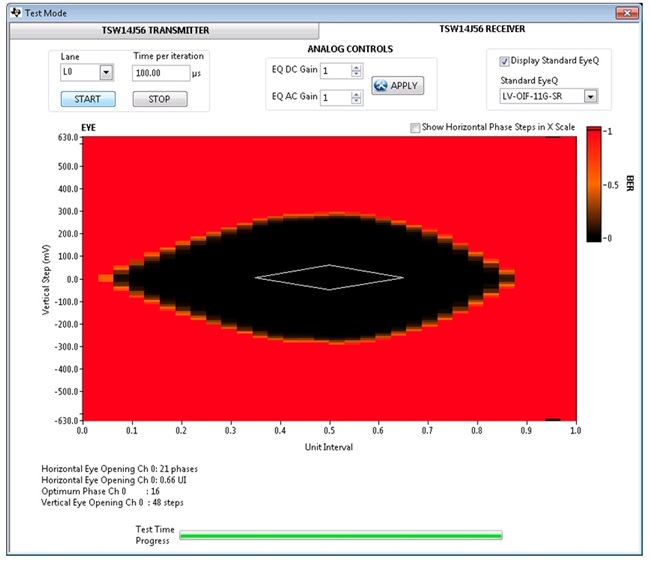
Figure 2 is an example of an open eye diagram acquired using the ADC12J4000 evaluation module (EVM) and TSW14J56EVM along with High Speed Data Converter Pro Software.
Figure 2: ADC12J4000EVM connected to TSW14J56EVM, both using high-performance materials, analog-to-digital converter (ADC) at 4GSPS in decimate-by-4 double-data-rate (DDR) P54 mode (data at 10Gbps) and a default pre-emphasis setting of 4d
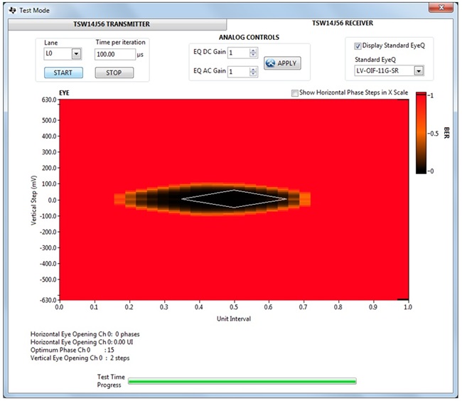
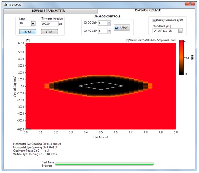
Figures 3 and 4 show the same baseline setup as in the open eye example, but with two different extender boards connected between the baseline EVMs. These extenders were added to evaluate the effects of longer links and lossier materials. Figure 3 is with a 16-inch trace extender board using Rogers RO4350B, another high-performance material. Figure 4 is with a 16-inch extender board using Isola 370HR FR4-type higher-loss material.
Figure 3: Baseline hardware plus 16-inch RO4350B extender board, 4GSPS in decimate-by-4 DDR P54 mode (10Gbps) and default pre-emphasis setting of 4d
Even with high-performance materials, long link distances attenuate the high-frequency signal components and begin to close the signal eye.
Figure 4: Baseline hardware plus 16-inch 370HR extender board, 4GSPS in decimate-by-4 DDR P54 mode (10Gbps) and default pre-emphasis setting of 4d
With a long link using the lower-cost material, the eye quality is severely degraded.
To restore the eye quality at the receiver, you must either select a lower-loss board dielectric or alternatively add some compensation at the serial TX/RX.
Many JESD204B TX/RX devices (ADCs, field-programmable gate arrays [FPGAs]) and digital-to-analog converters [DACs]) incorporate signal-quality compensation circuitry to mitigate the effects of high-frequency signal loss. ADCs will include pre-emphasis (boosting the high-frequency content) or de-emphasis (reducing the low-frequency content) features. On the receive side of the link, DACs and FPGAs may include equalization (adjust gain at different frequencies to optimize the equalizer output eye quality).
Using the TX pre- or de-emphasis feature can allow a system to operate with acceptable receive performance even with lower-cost FR4-type transmission media or longer-than-normal link distances. In these situations, the emphasis features are adjusted until the receive eye meets the specifications with some margin, but without excessive overshoot.
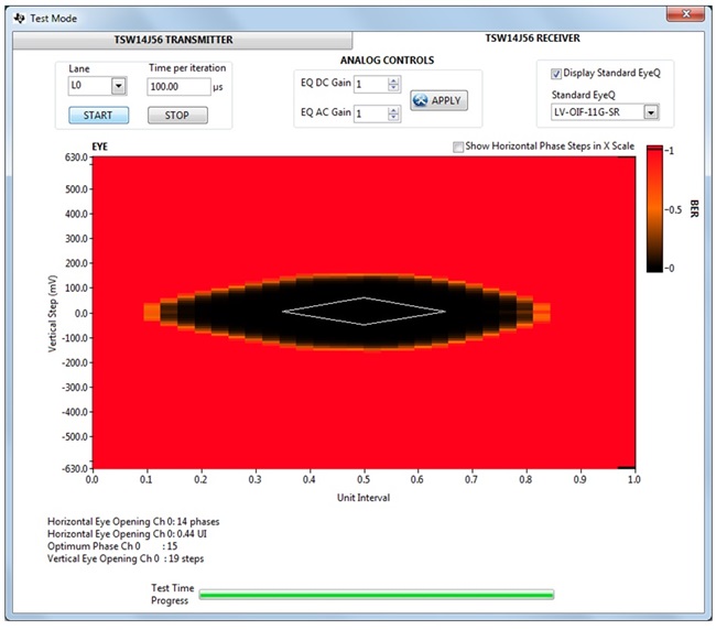
With the same extenders, the ADC12J4000 TX pre-emphasis settings were increased to optimize the data eye at the receiver. Figures 5 and 6 show the eye diagrams after optimizing the pre-emphasis settings for the high performance and FR4 type extenders. A significantly higher pre-emphasis setting is necessary to compensate for the additional loss of the lower-cost material.
Figure 5: Baseline hardware (ADC12J4000EVM + TSW14J56EVM) plus 16-inch RO4350B extender board, 4GSPS in decimate-by-4 DDR P54 mode (10Gbps) and pre-emphasis setting of 7d
Figure 6: Baseline hardware (ADC12J4000EVM + TSW14J56EVM) plus 16-inch 370HR extender board, 4GSPS in decimate-by-4 DDR P54 mode (10Gbps) and pre-emphasis setting of 15d
As I mentioned earlier, the input-signal and clock-signal paths can also drive the requirements of the board materials and stackup. Even if emphasis or equalization features permit link operation using lower-cost board materials, you may still need some higher-frequency layers to minimize signal-quality impacts for the analog or clock signals in a high-frequency design. You must consider all of these factors when selecting the board dielectric materials and planning the board stackup. Once you’ve made those choices you can design, build and test the system. In the testing and debugging phase of the design, you can adjust the TX pre- or de-emphasis settings and RX equalization settings to provide a reliable data link.
Additional resources:
- Read other blogs about designing with JESD204B.
- Learn about TI’s JESD204B ADCs, DACs, clocks and tools.
- Read our JESD204B white paper.


