Have you avoided multi-channel relay drivers because of EMI problems? This EMI problem can be solved by increasing the rise/fall time so that the circuit board traces to the loads do not act like transmission lines. Reducing the output slew rate will increase the rise and fall time. The driver slew rate can be controlled by adding a resistor (Rin) and capacitor (Cint) to make an integrator. Bam! Problem solved… here’s how to do it and typical results you will find:
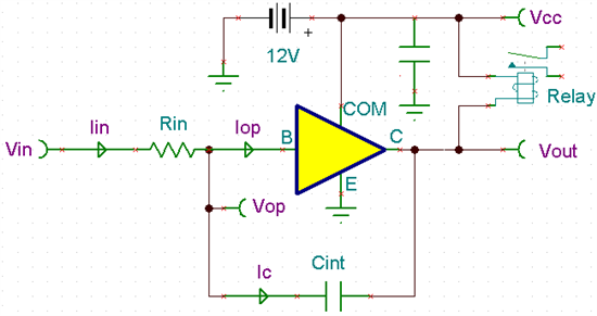
Figure 1: Schematic
Step 1: Approximate capacitor current based on the operating point of the driver
The driver input voltage (Vop) and input current (Iop) are nearly constant during the output slewing time. For practical values of input resistance (Rin), driver input current (Iop) will be much less than resistor current (Iin). So, capacitor current (Ic) can be approximated as being same as input current.
Step 2: Determine positive and negative slew rates
Positive output slew rate (input logic low) is (Vop - Vin) / (Rin * Cint) in V/S. Negative output slew rate (input logic high) is (Vin - Vop) / (Rin * Cint) in V/S. Divide by 106 to get V/uS . Iop and Vop vary with load and temperature. They can also vary device-to-device. Due to these variances, the rate control is good but not high precision.
For our experiment, we used Rin=402 ohms, relay is 12V with 122mA coil current, Vop = 1.7V, Iop = 90uA, Cint = [0.1nF, 1nF, 10nF, 100nF], VIH = 3.2V, VIL=0.1V, and here are the results:
Cint | Positive | Negative |
|
nF | Slew Rate | Slew Rate | Units |
None | 170 | 900 | V/uS |
0.1 | 25.9 | 33.4 | V/uS |
1 | 3.82 | 3.71 | V/uS |
10 | 0.376 | 0.379 | V/uS |
100 | 0.031 | 0.030 | V/uS |
Step 3: Use waveforms to verify results
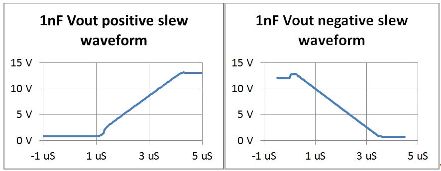
When RIN was increased to 1k ohms or 40pF of parasitic capacitance was added to driver input node there was a 30 to 40MHz oscillation on the positive slew waveforms. Therefore, the Rin and Cint should be close to the driver input pin to reduce trace capacitance, and Rin should be 402 ohms or less.

Step 4: Determine switching loss
The increased switching losses due to extended rise and fall times can be estimated using coil current, coil supply voltage, slew rate and frequency (average number of relay cycles per second: usually less than one). So, increased power loss is P = ½ * F * V2 * I / Pslew. For V=12V, I=122mA, 402 ohms + 10nF makes Pslew = 0.38V/uS, F = 1 (on/off) cycle/sec, power dissipation is just +23uW.
For a PWM application (to lower coil current during contact hold), the increased PWM power loss per channel is P = ½ * F * V2 * I * (1/Pslew + 1/Nslew). For V=12V, I = 70mA, 402 ohms + 100pF makes Pslew = 26V/uS, Nslew = 33V/uS, F = 25kHz, power per channel is +17mW.
So… Relay driver EMI can be reduced by adding a few passive components and a small increase in the driver’s power dissipation.
Does this solve your EMI issues?