Quantcast
Channel: Analog
Viewing all 585 articles
Browse latest View live

Analog basics: Beginner knowledge and veteran refresher

$
0
0

As a former college instructor who regularly lulled his students to sleep with a traditional lecture format, I’m excited to announce that TI is offering a “Hands-OnAnalog Basics” workshop at Design West 2013(April 22-25 in San Jose, Calif.)with our very ownamplifier expert, Art Kay!  This workshop is ideal for all analog engineers – from beginners to veterans – as well as digital designers and new college graduates.  Op amp topics from bandwidth to noise will be discussed, simulated, calculated, demonstrated andmeasured!

Everyone who attends the session will have their own workstation composed of a computer, National Instruments (NI) myDAQ, and multiple custom Texas Instruments (TI) experimenter boards.  Below is a picture of the hardware setup we’ll use to demonstrate common-mode voltage, output swing, slew rate and bandwidth during the session.

This hardware will correlate real-world results with theory and simulation.  The results from our output swing module are shown below.  Believe it or not, these results even correspond to the data sheet specifications!

                                TINA-TI Simulation                                                Measured Results

Each topic will start with approximately 15-20 minutes of theory (hopefully not enough to lull everyone into a deep slumber) before transitioning to interactive activities like running TINA-TI simulations and taking real-world data using the NI myDAQ.  In contrast to my higher-education days, this methodology transforms the experience from passive to active participation, which will increase comprehension and retention of the concepts presented.

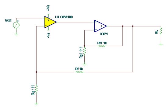
In addition to the aforementioned topics (bandwidth, noise, slew rate, common-mode voltage, and output swing), there are also modules that discuss active filtering and op amp stability.  The filtering module compares the Sallen-Key and multiple-feedback (MFB) topologies and shows the consequences of not selecting the right op amp.  The stability module shows you how to stabilize an op amp driving a 1uF load using an isolation resistor with and without dual feedback.  The selection of the topics was based on decades of experience supporting the design community, so the session should be very informative!

While I’m unable to be there in person, I helped Art develop this workshop and am thrilled to offer it at Design West 2013. I hope everyone who attends the session will find it to be rewarding, useful and fun!

Be sure you’re registered for Design West in San Jose, and then plan to attend one of our three “Hands on Analog Basics: Beginner Knowledge and Veteran Refresher” sessions in the Low-Power Design track: Monday morning (full session), Thursday morning (part 1) or Thursday afternoon (part 2).

Some browsers may experience compatibility issues when accessing information from the above links. If you’re not able to access thelinks, consider updating your browser or your version of Flash.


IAC or DIY? No, these aren’t stock tips!

$
0
0

IAC is what I call integrated analog circuits, some prefer AFE (analog front ends) while others would say IS (integrated solutions.) Whereas DIY has a universal meaning, “do it yourself!”

So the question now is, are you better off with an IAC over DIY, and why? It depends on the application, expertise, time to market, and total cost.

It’s almost like choosing a watch. Do you want it sporty or classy? Would you like a self winding automatic movement or quartz? How about crystal sapphire or hardened mineral glass? Or do you just want to know what time it is?

Consider an IAC in applications where several platforms could “reuse” the design with a quick spin. This is especially true for applications like temperature control and monitoring, weigh scales, and medical instrumentation, such as ECG/EEG and pulse oximetry. Most IACs are supported by easy-to-use software meant to help the system designer expedite a design and get a very good idea on the capabilities of these devices before deciding to prototype.  Some popular devices include the ADS1298 and ADS1299 for ECG and EEG respectively, the LMP9100 front end for gas monitoring and the AFE4400 complete sub system sub system for pulse oximetry.

On the other hand, there is always the DIY approach because of the 20nV/°C of drift which can only be accomplished by a super high precision op amp, such as the LMP2021. There are those looking for that 1nV which can only be found in a high voltage bipolar amplifier like the OPA211, and those who prefer analog-or digital filtering because that’s their secret sauce.

The choice is yours and you know your needs better than anyone, but the bottom line is more isn’t necessarily always better, if you’re racing the clock trying to put out a new product, then IAC is your best bet. If you’ve got room to spare on your board and want the highest quality product then perhaps a DIY approach is for you.

Let me know if an IAC or a DIY worked better for you. Or, ask questions and share knowledge with fellow engineers on the Support Forums in the TI E2E Community.  

Supercapacitors to the rescue

$
0
0

Monitoring the charging current of a supercapacitor application is very important.  Without a precision current limiter, the charging current can overshoot when the voltage of the supercapacitor charges quickly, thus damaging the system. 

To prevent this, try this method to precisely limit the charging current using the LMP8646, a precision current limiter used to improve the current limit accuracy of a load, like the supercapacitor.  This device can be connected to any switching or near regulator with an available feedback node. Many regulators might have an internal current limiter, but its output accuracy is often as high as 30 percent. The output accuracy of the LMP8646 can be as low as 3 percent, making it a preferred current limiter for many regulator applications.

The design for this supercapacitor charging application can be seen below in figure 1.  This example assumes the supercapacitor is 5F, and a limited current of 1.5A is desired. The LM3102 provides the current to charge the supercapacitor, while the LMP8646 monitors this current to make sure it does not exceed the desired 1.5A value. This is done by connecting the LMP8646 output to the feedback pin of the LM3102. This feedback voltage at the FB pin is compared to a 0.8-V internal reference. Any voltage above this 0.8-V means the output current is above the desired value of 1.5A, and the LM3102 will reduce its output current to maintain the desired 0.8-V at the FB pin.

Figure 1 – current limiting a supercapacitor

The LMP8646 requires external circuitries to limit the supercapacitor’s current. The sense resistor (Rsense) and gain resistor (Rg) are two components on the top of this list.  They both set the output voltage, which is connected to the 0.8-V feedback node.  Another key parameter to consider is bandwidth.  Operating outside of this recommended bandwidth range might create an undesirable load current ringing. For this application, a BW range between 500Hz and 3kHz is recommended.

At startup, the capacitor is not charged yet. Later, the voltage at the supercapacitor will change instantaneously, creating an overshoot of current that can be damaging to the supercapacitor. When the output voltage is at its nominal, then the output current will settle to the desired limited value. Because a large current error is not desired, ROUT needs to be chosen to stabilize the loop with minimal initial startup current error. In general, ROUT should be larger than 50 ohm. For this application, a ROUT of 160 ohm was chosen.

In summary, monitoring the charging current of a supercapacitor is very important.  The LMP8646 precision current limiter can do the job with an accuracy of 3 percent.  The design of the LMP8646 external circuitries consist of selecting the components for the voltage regulator, integrating the LMP8646 and selecting the proper values for its gain, bandwidth, and output resistor, and adjusting these components to yield the desired performance.

Check out my Engineer It video on the TI E2E Community to find out more information on how to limit the charging current of a supercapacitor. 

DAC Essentials: Static specifications & linearity

$
0
0

In my last post, “DAC Essentials: The pursuit of perfection,” I explained the concept of the ideal DAC and established the key idioms of its performance. Now we’ll explore how real devices deviate from the ideal DAC transfer function and how to quantify those deviations.

DAC specifications are divided into two basic categories: static and dynamic. Static specifications are behaviors observed at the DAC output at a steady output state, while dynamic specifications refer to behaviors observed during a code-to-code transition. When discussing linearity and the DAC transfer function, you only need to consider static specifications.

Let’s first start with a spec called offset error. Offset error describes how much the entire DAC transfer function is shifted up or down. The measurement is usually made from a line of best fit taken from a two-point measurement around 10% and 90% full-scale. We do this to avoid operating the output operational amplifier in the non-linear region near its power rails. If you were to consider slope-intercept form for a straight-line equation, y = mx + b, offset error would be the b term, as illustrated below.

Zero-code error is similar to offset error but describes a different and useful DAC behavior. Zero-code error is measured by loading the DAC with all 0’s and observing the DAC output voltage. In the ideal DAC, we would see 0V at the DAC output when loaded with all 0’s, but due to headroom requirements for the output buffer, we usually see some small offset from 0V.  

Another important specification is called gain error. As you may expect, it compares how the real DAC transfer function’s slope relates to the ideal slope. In the ideal case, the slope of the transfer function is equal to exactly 1 LSB, but frequently this figure is slightly off. The measurement for gain error is taken from the same two-point line of best fit used in measuring offset error. If offset error is the b term in y = mx + b, then gain error is the m term.

Offset error, zero-code error, and gain error are all provided holistically for a DAC using the measurement techniques mentioned above, which should make sense given what they’re describing. The remaining specifications, INL and DNL, are measured for each and every code in the DAC’s transfer function, but a single number is provided in the electrical characteristics table that expresses the worst case observed across the entire transfer function. The datasheet will also include graphs showing the typical INL or DNL across all codes in the typical characteristics section.

DNL is differential non-linearity. It expresses the difference between measured LSB size and ideal LSB size for any two sequential DAC codes. DNL is often used to infer DAC monotonicity and to determine if the DAC has any missing codes. Since most modern ADCs and DACs are monotonic, DNL is usually not as useful as INL.

The last static linearity specification is INL – integral non-linearity, which is also referred to as relative accuracy. INL describes the deviation between the ideal output of a DAC and the actual output of a DAC, where offset error and gain error have been calibrated out of the measurement. In a lot of ways, INL is the most valuable specification to consider for an application that requires extremely high precision. Offset, gain, and zero-code errors can be compensated for externally, but there is no way we can reach inside the device package and correct internal mismatches to fix INL.

In our next couple of posts, we’ll take a look at the DAC architectures used to create precision DACs. I hope you’ll check back for them in the coming weeks!

Leave your comments in the section below if you’d like to hear more about anything mentioned in this post or if there is a topic you'd like to see us tackle in the future!  

Commandments of RS-485

$
0
0

At TI, we often get questions about whether there are any quick tips or tricks to keep in mind when designing with RS-485. So, we've put together a comprehensive list of the top commandments to remember when working with RS-485. If you have any further questions on this topic, our team is always hanging out on our E2E forum, and we would be happy to help. So, without further ado...

The 14 commandments of RS-485

rs-485 designs

And how to apply them...

1) Use twisted pair cable with Zo = 120Ω or 100Ω

2) Connect bus nodes via daisy chain

3) Terminate unused conductors with RT = Z0 to their local grounds

4) Terminate one cable end with RT1 = Z0

5) Apply failsafe biasing to the other end 

6) Terminate this end 

7) Determine maximum cable length with chart bottom right

8) Make stub length no longer than 

9) You can operate 3V and 5V devices on the same bus

10) For ESD, EFT, and surge protection use SM712

11) Limit clamping current into the transceiver with 10-Ω pulse-proof or MELF resistors

12) Filter signal noise between transceiver and UART with R-C low-pass filters (fc ≥ 5 x DR)

13) For ± 7V GPDs use standard transceivers

       For ± 20V GPDs use SN65HVD17xx

       For higher GPDs use isolated transceivers 

14) Ask questions on TI's E2E Industrial Interface Forum.


Do you have your own tips? Share them with our readers below.

Turn up the heat

$
0
0

More and more electronics are needed for very harsh environments, which then results in the need for multiple electronic components.  For instance, oil and gas drilling, where temperatures reach up to 200°C require complete solutions for intelligent down hole tools to find and recover resources for energy production.

We’ve been working on high temperature integrated circuits (IC) for this market for several years and have developed a complete signal chain solution of microcontrollers, digital signal processer (DSP), amplifiers, data converters, power, and interface functions, but the one area missing has been non-volatile memory. Now, thanks to the SM28VLT32-HT, there’s a high temperature flash memory device capable of reading and writing up to 210°C.  This device eliminates the need for costly up-screening and qualification testing of industrial-grade components for use outside their standard operating range.

The SM28VLT32-HT has a capacity of 4-MBytes and is the industry's first high-temperature, nonvolatile Flash memory device designed for harsh environments.  It is qualified and tested across the entire temperature range to provide robust read/write operation over the device's operating life.  Designed utilizing our 180nm CMOS flash process, it is built on the same process technology that allows our ARM7 and motor control DSPs to operate at 210°C.

Since size is a big concern in many of these applications, the SM28VLT32-HT was designed from the ground up to support extreme temperatures.  It is also available as a Known Good Die (KGD) to support higher levels of integration into multi-chip modules. This use of a serial SPI interface simplifies design and packaging, and reduces pin count.

The availability of high temperature non-volatile memory will enable more capabilities in many harsh environment applications.  The HT Flash offers designers more options for reading and writing to memory at temperatures greater than 210°C and provides reliable solutions for logging data or storing programs.


Current feedback amplifier...how do I make it work for me?

$
0
0

Current feedback (CFB) amplifiers mostly belong in the realm of high speed amplifiers. There are lot of good application notes developed over the years that describe the operation and the main issues encountered when applying current feedback amplifiers to a problem.  Here we’ll try to summarize them in a few good words.

A CFB amplifier has one high impedance input (the non-inverting input), one low impedance input (the inverting input), and one output low impedance, as is represented below.  Note that for the purpose of this discussion, I will be ignoring the power supply pin and disable functions.

Figure 1: CFB internal elements

The voltage on the non-inverting input sees a high input impedance so as not to load the input.  The voltage on the non-inverting input appears on the inverting input as it passes through a buffer.  As the buffer is non-ideal, it will have a gain a(s) that varies with frequency with DC magnitude very close to 1V/V but typically 0.996V/V.  The buffer also ideally has output impedance equal to 0W.  In practice, the output impedance varies between a few ohms to a few tens of ohms.  I will also ignore the inductive component of that resistance as well for now.

 The intent for the buffer is two-fold:

1)      It forces the inverting node voltage to follow the non-inverting input.

2)      It provides a low impedance path for the error current to flow.

As the error current passes through the buffer it is sent to the output through a high-transimpedance gain stage.  Closing the feedback loop will drive the error current to almost zero in a fashion similar to the error voltage being driven to zero in a voltage feedback amplifier.

The only action left is to write the equation and interpret it.

  is the noise gain, and in the case of the non-inverting configuration shown, the signal gain as well.

The loop gain can be expressed as:

This is a very important equation for an ideal CFB  as it expresses the loop gain is proportional to the feedback resistance hence the feedback resistance is acting as the main compensation for CFB.  In effect, increase the feedback resistance and the bandwidth (BW) will decrease the feedback resistance, while increasing the BW.  In practice, it is not possible to reduce the feedback resistance below a certain value otherwise the amplifier will oscillate.

As long as  , the BW, is not proportional to the gain, the CFB is considered fain-bandwidth product independent.  In practice this is true to the first order as   .

CFB will also have a naturally high slew rate and low bias current.  The input stage is a buffer and provides as much current as it can until the internal transistors saturate.  This saturation happens much later than traditional differential pair input voltage feedback amplifiers (VFB).  That characteristic is very important and translates to much higher full power BW.

To conclude, CFB is not meant for every application.  They fit best in applications that are most affected by increase in noise gain and where limited BW (a few 100MHz) but where high gain is needed.  The CFB most likely is not used as the front-end amplifier as the VFB tends to do better due to lower noise. But as a second stage, they do offer a much better BW to quiescent current ratio than any VFB.  CFB also does better in summing application where several inputs are required.  In such applications, VFB’s BW will be limited by the noise gain.  The last application in which CFB is most useful is line driver, where typically high gain and high BW are required simultaneously but also have high output current and high slew rate.


DAC Essentials: String Theory

$
0
0

No, I'm not actually going to talk about particle physics today - though that would be cool...instead we'll be discussing the theory of the string DAC architecture. String theory!

The string DAC, sometimes referred to as the Kelvin divider or Kelvin-Varley divider after its inventors, is one of the most straightforward methods used to design a DAC. In its simplest form, the string DAC is just a series of equally sized resistors with a tap point between each resistor. Based on the digital code applied to the DAC, the appropriate tap point will be switched to the output buffer. This limited switch movement results in very low glitch energy, which my buddy Tony Calabria will delve into in a future post in this series. Ideally, each resistor will induce a voltage drop from the reference equal to 1 LSB. A simplified illustration of the architecture is shown below.

As resolution increases in the string DAC, the number of resistors required for the design increases exponentially. A n-bit string DAC requires 2n resistors, so in general a high-resolution string DAC would require a large IC package. That translates to 65,536 resistors for a 16-bit DAC, 262,144 for 18-bits, and 1,048,576 resistors for 20-bits! Cascaded segmentation techniques are sometimes used to reduce the number of resistors required, but for our purposes we will not consider segmentation, as architectural trends tend to hold true at the application level even if segmentation was implemented.

The accuracy of each resistor value directly determines linearity. If any resistor in the string isn’t the appropriate value, we’ll see poor differential non-linearity (DNL) at the code transition corresponding to that resistor. Also, the integral non-linearity (INL) of all subsequent codes would also be offset by the mismatch. Given the number of resistors in a typical string DAC design, it’s impractical to trim every resistor and as a result, we typically accept DNL errors to some extent. However, it is still highly desirable to maintain good INL so sectionalized trimming on groups of resistors is frequently implemented to overcome trimming every resistor, which presents itself as a “staircase” effect on the INL graph shown below.

A perk of the string DAC is that the input impedance looking in from the reference input remains constant except during instantaneous code transitions. Other data converter architectures, especially SAR ADCs, have dynamic loading conditions that make a reference buffer a requirement, while the string DAC is more forgiving. In general, however, it’s a good idea to buffer any reference – especially if the input/output will change with great frequency. It’s also important to note that the equivalent input impedance from the reference is typically very high, making most string DACs very power efficient.

The final and most subtle element of the string DAC design is the divider present before the string resistors and tap points. This resistor is equal to the equivalent impedance of the rest of the resistors in the string and effectively halves the reference input. This is done in an effort to lower the common mode input requirements of the output buffer and help keep the cost low while delivering good performance. To compensate for this, the output buffer is typically in a non-inverting gain of 2 configuration, though sometimes the feedback resistor can be digitally controlled to realize different gains.

A few things to remember about string DACs:

  • Low cost via simplicity of design
  • Low glitch energy
  • Inherent monotonicity
  • Low power consumption

The string DAC frequently finds a home in portable battery powered applications that can make great use of its low power consumption. Additionally the string DAC is used in applications like closed loop control systems that leverage its inherent monotonicity and in low-cost applications where the DAC is providing some calibration feature to a system, rather than being the ‘star’ of the show as we may see in other DAC applications. If a string DAC sounds like something that interests you be sure to check out a few TI string DACs such as: DAC8562, DAC8560, DAC8568, DAC7678, DAC8411, DAC8718, or DAC8728.

For a refresher, check out previous posts in this series: series introduction, the ideal DAC , and static specifications and linearity. In our next post we’ll continue the discussion of DAC architectures with the R-2R DAC and MDAC.

Leave your comments in the section below if you’d like to hear more about anything mentioned in this post, or if there is a topic you would like to see included in future posts! 


Addressing those pesky European power consumption rulings

$
0
0

This January, the European Commission implemented legislation to limit the power consumption in line-powered products when they are deemed in "standby" and "Off" mode.

Traditionally, home audio products were guilty of wasting a lot of power. My teen years were spent hearing my parents tell me constantly that "The TV is still burning power with the screen in standby!! Turn it off at the socket!" Thankfully, British power sockets have individual switches at the wall. But that's another blog post entirely ;).

The latest EcoDesign legislation in Europe has demanded that products consume less than 500 mW in standby. That sounds easier than it is, as most off-the-shelf external power adaptors can burn 300 mW when idling, leaving the system with 200 mW. Add to that the idle power consumption of audio amplifiers, and you’re soon in trouble.

Smart folks out there have used DSP's and other processors to detect when audio sources have been removed, and can put the product in standby-mode. This can be done either in the DSP, or in an analog circuit along with some assistance from the system microcontroller. This is a great way to make the product "go to sleep," but in many cases, the challenge may be "waking up." Once your DSP has been powered down, you no longer have the ability to monitor and "wake up."

Multiple other solutions are possible, including some that integrate comparators with peak hold circuits to detect a threshold. These are typically rather large, and require pretty accurate resistors to set accurate threshold points above your noise floor to guarantee error-free signal detection.

The types of signals that we need to detect have changed, as well. Traditionally, we only worried about the analog signal. Now that we have data coming from wireless modules, HDMI and S/PDIF, we need some intelligence on how we detect. By using "lock" as a trigger to have a quick look (Figure 1) to see if the audio data pin in the I2S stream is toggling high and low, you can "see" if there really is quality data, or if it’s just a string of zeroes. 

 Figure 1: Use “lock” as a trigger to see if the audio data pin in the I2S stream is toggling high & low.

TI has a number of solutions integrated into its products that can do this, such as the PCM9211 digital audio interface transceiver, but if you want to implement them discretely, here are some tips (and please use TI silicon).

ANALOG: Use the system MCU's spare ADC, precondition the input with an analog peak hold circuit and wake up the MCU every second or so, do an ADC conversion, then go back to sleep.

WIRELESS MODULE: Leave the wireless module in pairing mode, and look for the "Lock" signal. Danger: Some devices can lock, but receive zero data. Consider treating it like an I2S source, see below.

S/PDIF Receiver: Leave the S/PDIF device on (it’s a low power consumer), look for the "Lock" signal. Danger: Some devices can lock, but receive zero data. Consider treating it like an I2S source, detailed below.

I2S Source: Look for data toggling on the data pins. Ideally you'd process this data with a DSP to check the amplitude, and if it's relevant data... but toggling SDIN data is a sign that there's activity. You may choose to wake the DSP once you detect LOCK and DATA.

Being negative can still be positive

$
0
0

The first operational amplifiers (op amps) used what is commonly called split power supplies, meaning the power for the amplifier was symmetrical around ground with both positive and negative polarities.  Since most power supplies used transformers to convert 120 V mains electricity, a simple center tapped secondary winding gave easy access to a negative power supply. 

Today, many devices now run on battery power, and even mains powered equipment is trending towards having only positive power supplies. But, I don’t recommend ruling out having a negative power supply. 

Many signals are still ground referenced and carried on coaxial cables.  High performance components, like analog to digital converters, may run on 1.8 V power supplies and require an input signal centered at 0.9 V.

Even the lowest threshold MOS technology cannot generate signals that are truly rail-to-rail and the base-to-emitter voltage (Vbe) on bipolar technologies has not changed significantly from the 0.6 V commonly associated with silicon PN junctions.  This means that if an amplifier is going to recreate a signal that swings close to ground, or even more difficult, is ground referenced, a negative power supply is necessary.

Fortunately, generating a negative power supply is very inexpensive, especially if the current requirements are low.  A device like the LMR70503 SIMPLE SWITCHER can generate a negative power supply with only 7 external passive components. 

The LMH6554 is a differential amplifier designed for both single supply and split supply configurations.   Using the LMR70503, an existing  3.3V supply, can be converted to a +3.3 V and   -1.7V split supply.   With this supply configuration, the LMH6554 output voltage can now swing from  -0.6 V to +2.2 V.  This range is adequate for driving most analog-to-digital converters and many ground referenced signals such as composite video.  Other combinations of supply voltages, like +4 V and -1 V would be ideal for an ADC such as the ADC081500 shown below. 

With the advent of switching power supplies there is no reason to limit yourself to only positive power supplies, even when designing battery powered equipment.  Don’t be afraid to specify a negative power supply in your next high system design. 

Let’s take this driver out for a spin

$
0
0

Before I suggest a suitable op amp to drive an ADC, I look at the application. This steers me toward one of two categories: low voltage or high voltage.

If the system requires a low voltage operation, chances are I’ll look for a low power op amp. Depending on how low the power needs to be, I may also look at a few different options in addition to the input stage and the building process. That’s because not all low voltage op amps have a CMOS input stage. Conversely, if the application is sensitive to noise and the goal is to optimize for dynamic range, I’d look at the 30-V or higher, such as the OPA211 , though sometimes 24-V like the LM6211 will work. But, this isn’t enough.

You also need to consider the output drive capability of the op amp. This can lead to some reluctance, especially in low power designs, as you may think that your micro power amp will never have enough juice to drive the input stage of your ADC. In reality though, it comes down to the biasing and the design of that particular amplifier. Some have a very robust output drive even with very little quiescent current, such as the LMP2231. This is where design talent comes into play; it depends on how much of the bias current is diverted to the output stage.

Of course all along you’re also looking at the DC specifications of your op amp to make sure you stay within the acceptable boundaries of the design. But how many people look at things like settling time, I wonder! This is an important parameter, and can really hurt your conversion time if you’re not careful.

I sometimes hear someone say “oh, no problem with settling time, I just look at the widest possible bandwidth and I know that will have a faster settling response.” Well yes and no.

Yes, because bandwidth gives an indication. No because it isn’t enough. What settling time also depends on phase margin as well as the location of the poles and zeros, be them intrinsic to the op amp or external.

So next time you’re looking to take a driver out for spin check out the OPA320, settle within 0.5us at 16 bits and use it with the ADS8319. You’ll be the first one to the checkered flag!! 

Filter for thought

$
0
0

Have you ever wondered how engineers designed active filters before the birth of software? They were able to do it using nomographs - but before we talk about what these are, let’s refresh our memory a little bit on active filters.

Magnitude is the amplitude of the output. Phase is the angle of the output. Every pole adds -90° at high frequencies. Theoretically, a fourth order filter would phase shift through 360°, though the magnitude would be very small.

Group delay, on the other hand, is the derivative of phase with respect to frequency. It’s a measure of the time delay (filter’s time) in frequency. A filter with a flat group delay means that the output signals come out with the same relative phase as the input signals. In essence, everything is delayed by the same amount.

Before you decide on your filter design consider the tradeoffs between the various implementations and types. Let’s review a few important ones:

Narrower transition regions require higher filter order filters. That is, you’ll need a higher component count - active and passive. If you can tolerate more ripple in the passband, you can get a smaller transition region for the desired attenuation. However, a monotonic passband  gives you a smoother phase response which yields a constant group delay in the passband, important in multi frequency communication.

Now that we touched on some of the tradeoffs, let’s take a look at some of the most common types of active filters.

  • TheButterworth has a monotonic passband and stopband. It’s optimal with respect to passband ripple, also known as maximally flat but has a wide transition region. It’s often chosen for anti aliasing.
  • The Chebyshev has an equal amount of ripple in the passband and a monotonic stopband, providing a fast transition region.
  • The Elliptic, sometimes referred to as a Cauer filter, has equal-ripple in both the passband and the stopband and gives you the fastest transition band of any filter. It does, however, have a long tail of settling time and requires a more complex implementation including poles and zeros in the transfer function.
  • The Bessel, also known as Thomson filter, offers the most constant group delay in the passband. It’s optimal with respect to group delay and is also called a linear phase filter, not to be confused with zero phase. The Bessel has a monotonic passband and stopband but has a wide transition region.
  • The Inverse Chebyshev gives you a monotonic passband and equal ripple in stopband, with the same transition region as the Chebyshev .  

Take a look at figure 1 below to see the different filter bands described above.

Figure 1. Representation of different filter bands

So now what about those nomographs?

Suppose you want to design a low pass filter, assuming an active filter with -3dB at 300kHz and -60dB at 1.2MHz. Once you’ve decided which filter type you’re going to use, you’ll need to determine the minimum filter order.

Suppose you want to design an anti-aliasing low pass filter where your goal is to minimize ripple. You’ll need to look at the Butterworth nomograph and follow these steps:

  • Determine Ω= ΩSP
  • Extend a line to connect between  MP and MS
  • Draw a horizontal line across graph to intersect Ω
  • The higher number represents the minimum filter order

In this example, you’ll need a fifth order.

If you plug the same numbers into FilterPro, you get the same answer. See the below figure.

Suggesting a “good” op amp for an active filter is not a trivial task and depends greatly on the implementation as well as the application. If you have a low voltage design and are in need of good settling time and low ripple the OPA320 is a good candidate.  If your design uses higher voltages and requires good linearity consider the LMP8671 or OPA211.

For more info on how to ensure measurement set-up is properly calibrated and matched to avoid measurement errors due to ripples check out Habeeb Ur Rahman Mohammed’s “How to understand ripples in RF perfomancesEngineer It video.

RS-485 - Who says you can't teach an old dog new tricks?

$
0
0

Would you agree that RS-485 has turned out to be one of the most versatile communication standards when it comes to industrial applications? It’s very reliable for long distance communication and very popular. In all the years that the RS-485 standard has been around, RS-485 transceivers have undergone a lot of changes. Just like we crave more "apps" on our phones, RS-485 users want more features in the transceivers making it safer and robust.

With safety and protection in the forefront for industrial applications, transceivers today have a bunch of safety features packed into the same package. If you fear the common-mode voltage in your system is going to violate the standard (-7 to 12V), then simply choose one that has two times wider common mode range, such as the SN65HVDHVD20. By the way, we call these SUPER-485 devices because they are the true super-stars when it comes to industrial applications/harsh environments where there is likelihood of ground movement.

For cases when there is a possibility of over-voltage faults due to accidental shorting of wires to power supplies or mis-wiring, one could use transceivers, such as the SN65HVD1780, which are high-voltage fault protected. As long as the voltage on the bus lines in not greater than 70V, the device will survive. Once the fault is corrected, the system will work as expected.

Lastly, if there is clutter on the board surrounding the transceivers such as ESD diodes or transient voltage suppression (TVS) diodes, why not clean them up with the SN65HVD72 family or the SN65LBC184 devices? These devices, especially the SN65LBC184, will ensure that a lightning strike does not damage your transceiver. Yeah, it's that robust; we call it our SUPER-DUPER485.
 
Oh!! Did I mention each of these transceivers is backward compatible to the basic RS-485 transceiver without any frills? So upgrading your old solution should be as easy as hitting the easy button at Staples. Well, maybe not, but as easy as un-soldering the old device and soldering in one of these super-stars. Then watch your old RS-485 system breathe a new robust life.

Cable equalization 101 – Automating your design

$
0
0

Judging by the number of views on a post related to numerical cable equalization, on the High Speed E2E forum (more than 3,700 at last count!), I would guess that it’s a pretty interesting topic for many folks. Since TI is one of the leading manufacturers of current feedback amplifiers (CFA), the workhorses for cable equalization, this two-part blog is devoted to giving you everything you need to implement your custom design, with a list of best devices to use and simulation techniques to boot. In this post, I will present some background information on equalization and a spreadsheet that allows you to automate the design. In part 2, we will use TINA to simulate the design and look into methods of improving the stability of the stage.

Xavier Ramus, a frequent contributor to Analog Wire, does a great job in his Application Note, A Numerical Solution to an Analog Problem, of explaining how to use a spreadsheet like Excel to do the hard work of placing the poles and zeros of Figure 1 high frequency (HF) gain boost banks (RA, CA, etc.) at the right frequencies to match the cable so that the cable + amplifier exhibits a flat frequency response. The reason this task is not trivial is these poles and zeros interact with each other if they are spaced close enough, making it difficult to “tune” the total arrangement. With the spreadsheet you can manipulate the component values and see their effect instantaneously.

Figure 1: Typical equalizer schematic where RA, CA, etc. boost gain at high frequency


In the below Excel file, I have implemented the spreadsheet that Xavier has explained. It is set up for four boost banks (R_1, C_1 through R_4, C_4) capable of 25dB of boost. For more boost or longer cable lengths, you can cascade more identical stages. The spreadsheet has an entry for the number of stages “N” in cell M6, default set to “2”. This enables you to increase the total boost (e.g. 50dB of boost for two cascaded stages, etc.) for longer cables. For additional information, check out the below PowerPoint.  

(Please visit the site to view this file)

(Please visit the site to view this file)

Earlier I mentioned that CFA is the architecture of choice for an equalizer. The reason is that the high frequency noise gain (1+RF/ZG where ZG is the total impedance from the inverting input to ground) increase that you need for equalization has much less unwanted impact on loop gain (and subsequently closed loop response) for a CFA than for the traditional voltage feedback topology. Furthermore, a CFA with lower internal buffer output impedance (RI,see OA-13) holds an advantage because of the same reason. Table 1 below is a list of TI CFA amplifiers with pertinent specs, ordered from lowest RI to highest:

Device

Devices / Package

RI (Ω)

RF nominal (Ω)

Large Signal BW (Av=+2)

(MHz)

Slew Rate (V/µs)

Max Supply Current / channel (mA)

Supply Rails Range (V)

Output Current (mA)

Packages

TINA Model?

1k price ($)

THS3201

1

11

768

880

6,700

18

6.6-15

100

SOT23

SOIC-8

VSSOP-8

MSOP-8

Y

1.95

THS3001

1

15

1k

300

6,500

9

9-33

120

SOIC-8

MSOP-8


Y

3.38

OPA695

1

29

402

450

4,300

13.3

5-12

120

SOT23

SOIC-8

VSSOP-8

Y

1.48

OPA2695

2

29

402

400

2,900

13.3

3.5-12

120

SOIC-8

QFN-16

Y

2.98

LMH6733

3

30

390

1,000

3,750

7.3

3-12

80

SOIC-16

Y

2.47

LMH6738

3

30

549

400

3,300

11.7

10-12

90

SOIC-16

Y

2.60

OPA694

1

30

402

675

1,700

6

7-12.6

80

SOT23

SOIC-8

Y

1.38

OPA2694

2

30

402

670

1,700

6

7-12.6

70

SOIC-8

Y

2.58

LMH6703

1

30

560

750

4,200

12.5

8-12

90

SOT23

SOIC-8

Y

1.35

OPA3695

3

37

402

440

1,700

13.3

3.5-12

120

SSOP-16

Y

3.73

LMH6714 / LMH6722

1/ 4

180

390

400

1,800

7.5

10-12

70

SOT23

SOIC

TSSOP

WSON

SOIC

Y

0.73 1.41

LMH6723/ LMH6724

1/ 2

500

1.2k

100

600

1.4

5-12

110

SOT23

SOIC-8

Y

0.79/ 1.00

LMH6702

1

N/A

237

720

3,100

16.1

10-12

80

SOT23

SOIC-8

Y

1.45

Table 1: TI High speed CFA portfolio


Once you’ve selected a proper device from Table 1, enter its recommended feedback resistor “RF nominal” value in Excel cell C6. To get your design (Excel row 6 final values), follow the instructions in the PowerPoint file (pages 4-9) and use Excel Solver function to minimize the difference between the computed response of your amplifier from the computed attenuation of your cable (the Excel file is already set up for that in Column P). You can find “minimize” (called “min”) in Excel under data > solver. The solver function does this by manipulating the values of gain elements in row 6 to find the best solution. You do this at low frequency and work your way up to the highest frequency of interest, and when you’re done you will end up with a plot in Excel, such as the one in Figure 2 where the amplifier response overlaps the cable attenuation plot (up to 100MHz and with ~55dB of boost from 2 identical cascaded stages).

Figure 2: Amplifier gain superimposed on cable loss

This allows you to equalize the losses in your cable for a flat overall (cable and amplifier) response. Figure 3 shows the schematic of the circuit designed by Excel:

Figure 3: Excel Solution_ One of Two LMH6733 Stages Used as Cable Equalizer


Stay tuned for Part 2, where I will discuss how TINA can be used to simulate this circuit in order to shed more light on its stability. In the meantime, please use the comments field below to fill me in on some of your biggest challenges with numerical cable equalization. Also, let me know if you found this useful and if there is additional information you feel I should cover in Part 2 of this 101. 

This amplifier doesn't exist...now what!?

$
0
0

Sometimes it’s impossible to find an amplifier with the right input and output characteristics, but a signal chain approach described in my previous blog posts on high gain, high bandwidth works well. Although very high gain can be achieved, one limitation of this approach is the limited DC accuracy.  For application where DC accuracy is a must have, creating a composite amplifier is the best approach.

A composite amplifier is an amplifier made of separate elements with non-ideal properties where the end result takes the best of both elements and combines them together.  Let’s consider the first amplifier, the OPA188.  It is an excellent auto-zero amplifier, but has a major limitation in that its gain bandwidth product is only 2MHz, limiting both the maximum gain and the achievable bandwidth.  Auto-zero amplifiers are usually used in high gain application with very limited bandwidth where excellent DC-accuracy, and in particular, offset drift is necessary.  The high gain requirement by itself increases the DC accuracy requirement.  The open-loop gain characteristic of the OPA188 is shown below in figure 1.

Figure 1: OPA188 open-loop gain and phase

To create the composite amplifier, I added a second stage using an ideal amplifier to the OPA188, see figure 2 below.

Figure 2: Composite amplifier with OPA188 as first stage and ideal amplifier as 2nd stage

The second stage, when placed in the loop of the OPA188, will increase the open-loop gain by its gain.  Note that I have opted to use 20dB for the second stage.  I have also placed the composite amplifier in a non-inverting 20dB gain configuration.  The resulting open-loop gain and phase of the composite amplifier can be seen in figure 3 below.

Figure 3: composite amplifier open-loop gain and phase

The composite amplifier will now have higher slew rate and higher gain bandwidth product.  You will also notice that it is not going to be unity gain stable any more but must be operated at a minimum gain. Since the second stage is ideal, it will not introduce any phase shift in the phase of the composite amplifier.

Stay tuned for my next blog where we’ll cover the selection of the second stage and evaluate the performance of the entire circuit. In the meantime, check out my high gain, high bandwidth series that will hopefully help you solve some design challenges.

High gain, high bandwidth…how can I get it all?

High gain, high bandwidth…why is this circuit oscillating?

High gain, high bandwidth…putting it all together


DAC Essentials: The Resistor Ladder

$
0
0


In my last post, I discussed the string DAC architecture and its tendencies― if you missed it you can view that post here. This post will focus on two very similar architectures, the R-2R DAC and the MDAC.

Recall that the big limitation of the string DAC is the challenge associated with realizing a high resolution design and maintaining linearity. The number of resistors required for the string DAC increases exponentially as resolution increases, unless clever design tricks are implemented like cascaded resistor strings or interpolating amplifiers. The R-2R architecture directly addresses this problem by utilizing a binary weighted resistor ladder structure, illustrated below;

Each bit of resolution of the DAC is made of one set of R resistor, 2R resistor, and 1 switch that moves between the reference voltage and ground creating a voltage divider at the output node. Typically there is an on-silicon output buffer included. If you’re having a hard time understanding how the binary weighted divider works, I recommend creating this circuit in TINA-TI where you can simulate each switch position.

The R-2R DAC sees a variable impedance at the reference node, so a reference buffer is a requirement for applications where the DAC output is going to be changed very frequently in order to keep reference settling time from impacting DAC output settling time. Usually this buffer is included on silicon, just like the output buffer, but make sure you consult your device’s datasheet before making any assumptions.

The MDAC, or multiplying DAC, uses a very similar topology – the same R-2R ladder in fact – except that the position of the reference input node and the output node are swapped. This change makes the R-2R ladder a current divider rather than a voltage divider. Because of this a transimpedance output stage is required to convert from current output to voltage output. Typically this buffer is not included on silicon but the feed-back resistor required for the transimpedance stage is included. Featuring the feedback resistor on silicon helps to ensure resistor matching to the rest of the R-2R ladder in terms of both value and drift behavior.

Not including an output buffer may seem like a disadvantage to the MDAC but in many ways it is actually quite helpful. Moving the amplifier to outside the device allows for great flexibility in design, applications with relaxed requirements can choose cheaper amplifiers and save money versus the price of a fully integrated solution. Meanwhile, in high-performance systems it is beneficial to utilize discrete amplifiers that are made on strong pure-analog processes.

As far as performance tendencies go, the R-2R and MDAC architectures have very similar properties and we’ll discuss them simultaneously.

Since there are fewer resistors in these designs we can implement a much more comprehensive trimming scheme to achieve very strong linearity. Trimming circuits also take up space, though, so the R-2R and MDAC packages tend to be larger than the string DAC.

The number of switches moving in the R-2R and MDAC designs is code-dependent. In some cases, every switch of the DAC may have to move to increment to the next code which will create much higher glitch energy than the string DACs.

Some things to remember about the R-2R DAC and MDAC:

  • Excellent INL/DNL
  • Medium to high glitch energy
  • Larger packages

The R-2R and MDACs find homes in virtually any application that is very high performance. That includes industrial programmable logic controllers, automated test and measurement equipment, precision instrumentation, and various other applications. Since the MDAC does not feature reference or output buffers it can deliver good results in medium speed applications as well such as waveform generation or AC attenuators. If these devices are of interest to you be sure to check out a few TI R-2R DACs and MDACs such as: DAC8811, DAC8822, DAC8734, DAC9881, DAC8881, or DAC7654.

This post finishes out the discussion of the DAC basics. Tony Calabria will continue the series with a deep dive into glitch and glitch reduction in the next few posts so stay tuned.

As always, leave your comments in the section below if you’d like to hear more about anything mentioned in this post, or if there is something you would like to see included in a future post!

Ditch the NTC thermistor: use an analog temp sensor

$
0
0

NTC thermistors and analog temperature sensors are two commonly used temperature sensing solutions that can be used for most electronic applications.  Deciding which technology is the best fit for your application can be a difficult task.  However, I’m going to show you a few reasons why you should ditch the NTC thermistor and design in an analog temperature sensor.

Figure 1 shows an output voltage vs. temperature comparison.  Notice that NTC thermistors require the use of a resistive network in order to help linearize their output.  This is because their resistance vs. temperature characteristic is exponential.  Unlike NTC thermistors, analog temperature sensors do not require any additional components as they have a virtually linear output voltage.  For example, Texas Instrument’s LMT87 analog temperature sensor provides a virtually linear output voltage across the devices entire operating temperature range of -50°C to 150°C.

As you can see from the three NTC thermistor curves in figure 1, you can change the value of the bias resistor to adjust the location of the linear portion of the curve.  Notice that this is a limited range and that the curves start to saturate at low and high temperatures.  When interfacing with an ADC, this saturation will cause temperature errors if the resolution of the ADC is not high enough to detect a change in output voltage per degree Celsius.  As a result, NTC thermistors tend to be less accurate across the entire operating temperature range and often require a higher resolution ADC.

Figure 1: Output Voltage (V) vs. Temperature (°C)

Figure 2 shows a supply current vs. temperature comparison.  The LMT87 has a typical value of 5.4µA and a max value of 9µA.  NTC thermistor networks tend to dissipate more power as their supply currents are much higher and vary greatly over temperature.  Notice that if you increase the resistance of the bias resistor, the supply current for the NTC thermistor network will decrease.  But remember, the bias resistor is also chosen to ensure that the output voltage vs. temperature curve is linear for the desired temperature range.  This is a tradeoff that can be ignored by using an analog temperature sensor as they have both a fairly constant low supply current and a virtually linear output voltage.  Another disadvantage to NTC thermistors is that engineers must account for the self-heating effect as this will cause additional errors.

Figure 2: Supply Current (µA) vs. Temperature (°C)

You can avoid these NTC thermistor design issues by ditching them in favor of TI’s easy-to-use analog temperature sensors. Check out my Engineer It video on the TI E2E community and learn more about TI’s analog temperature sensors.  

Cable equalization 101 - Simulating the design and improving stability

$
0
0

In “Cable Equalization 101 - Automating your design,” we saw how a spreadsheet like Excel can be used to generate an equalization design rather painlessly, and we obtained the design in Figure 1 below. Here, we will use simulation to make sure the design is stable.

Figure 1: Excel solution found in Part 1_ one of two LMH6733 stages used as cable equalizer

Since Excel doesn’t know about the non-ideal behavior of the amplifier you have chosen, it is wise to test the results of the equalization design using simulation. Without a good simulation model for the cable, one would have to rely solely on the amplifier open loop response simulation. It turns out we have the means to investigate this stability criteria for the CFA in TINA as explained further below.

From OA-13, CFA Loop Gain Analysis, the CFA transfer function shown below in Equation 1, the stability criteria states that at the frequency where Z(s) (Transimpedance Gain) intercepts Feedback Transimpedance (Rf + RI (1+ Rf/ Rg)), the phase shift should be 135˚ or less (for 45˚ phase margin). We can investigate this intercept point in TINA to increase the confidence in the design.

Equation 1: CFA transfer function

For a cable equalizer, replace Rg in Equation 1 with the complex impedance ZG, which is the parallel combination of all boost bank elements, R1, C1, R2, C2, etc., (including RG) shown in Figure 1. We rely on the amplifier (LMH6733) TINA file to model the behavior of Z(s) over frequency and also the fixed value of RI built into the model. And of course Rf is the recommended feedback resistor for this particular CFA, which is what was used in the Excel file to produce the Figure 1 solution to begin with.

Here is how we can get these pertinent plots over frequency to show in TINA for us to conduct our stability analysis:

a)      Feedback Transconductance (1 / Transimpedance) is the current flow into the inverting input (I_Rsense) in response to output (OUT1), with the loop open. Figure 2 below includes L_Large and C_Large which open the loop in AC (where we are concerned about stability and response) but leave it closed for DC to set the operating point.

b)      Z(s) is “Amp_out / I_Rsense” (TINA can easily do the arithmetic on waveforms!)

Figure 2: TINA tricks to open the loop and to sense inverting current

So, we have everything at our disposal to investigate the point of intercept of Z(s) and feedback Transimpedance graphically using TINA. See Figure 3 below for three values of resistance R1, chosen as the bank element most likely to affect stability, in order to find the optimum value of R1.

From Figure 3, the direct Excel solution (R1= 1ohm) would be unstable because of the 40dB/decade rate of closure of the two plots (this has to do with excess phase shift around the loop). Increasing R1 to 50ohm would be excessive and would limit the frequency response, while R1=10ohm is ideal because it places a Feedback Transimpedance pole at the intercept frequency and yield about 45˚ of phase margin.

We were able to take the Excel design one step further and verify against the device’s TINA model to anticipate real world issues with the boost in noise gain we have implemented. Bench verification and optimization of the design with the actual intended cable is the next step to complete the process.

I’ve included the TINA simulation file link for those of you who like to tinker with it and test other possibilities.

(Please visit the site to view this file)

Hope you enjoyed this blog and found it useful. Please let me know if there any questions!

Also, if you ever do a similar stability analysis on a voltage feedback amplifier, check out my two-part article on “using Pspice to analyze amplifier loop stability – part one and part two.”

Engineering the world through Analog

$
0
0

Our lives are surrounded by analog everywhere we go. That’s not news to the Analog Wire audience, but it may surprise some that in this age of digital electronics, analog technology is more pervasive and impactful than ever. In everything from power tools to a runner’s heart-rate monitor to the factory robot, analog chips are managing batteries or power from the wall, converting and conditioning signals, and providing the system interface. Technology has made and will continue to make an impact on the way we live, learn, work and play.

Just take a look at the advancements our customers have introduced recently or are on the horizon in the automotive and industrial markets, from cars that correct driver errors to avoid accidents to a factory production line that diagnoses itself to avoid shutdowns. One example that excites me is the automotive camera system. These megapixel camera systems serve as an important safety feature by allowing the driver to see what’s behind the car when in reverse, as well as around the vehicle in other types of driver assistance systems.

With TI’s FPD-Link III products the customer can connect all those cameras with only a single coaxial cable, instead of commonly used shielded twisted quad (STQ) or similar wiring. The impact is significant! The complexity of the car wiring harness is reduced by reducing the number of cables and connectors, which reduces the OEM’s manufacturing cost. Also, the driver benefits as the reduced weight (half that of a STQ), which translates directly into lower fuel consumption. Here’s a block diagram that details the system.

Analog and embedded processing technologies are the backbone of many of these inventions. And, because we see innovation through the lens of our 100,000+ customers who are changing the world right now, we have a unique vantage point.

Every few years, an undercurrent of technology drives the creation of products that change our lives. Just a couple of decades ago mobile phones enabled us to talk to anyone on the move. The Internet opened up the world’s knowledge base to anyone with a connection. Now we can access virtually any information, regardless of where we are, in real time on a host of different devices. Countless new uses have spawned from these advances, such as crowd sourcing, social media, cloud computing and many others. The possibilities are endless!

Futurists may be able to predict where the next wave will go. In our 83 years as a company, we at TI have learned to focus on what we do best. We provide the tools in the form of analog and embedded processing semiconductors and applications support that help our customers create the next big idea.

In my next post, we’ll discuss some of the innovations we are seeing in industrial automation, health technology, automotive and smart energy and ask you to be the judge of which applications will change our world in the coming decade.

This amplifier doesn't exist...now what?! - Part 2

$
0
0

In Part 1 of this post, we looked at the theory involved in making a composite amplifier, but we had yet to replace the ideal amplifier with a real component. Here we will discuss the physical implementation of the second stage.

A current feedback amplifier (CFA) would be ideal for this role.  For a quick refresher on CFA’s and how to use them check out my previous post titled “Current feedback amplifier...how do I make it work for me?

For this high DC precision and high speed composite amplifier, we will select the OPA684 because it has a low quiescent current of 1.7mA, but can achieve excellent bandwidth at high gain.  This allows us to optimize the gain bandwidth product (GBWP) of the composite amplifier while maintaining reasonable power consumption for the solution.  The OPA684 GBWP is shown below for reference.

Figure 1: OPA684 gain bandwidth product

The circuit with the OPA684 in it is shown below in figure 2.

Figure 2: Composite amplifier with OPA188 as first stage and OPA684 as second stage.

The operating voltage of this solution is limited by the minimum and maximum operating voltage of either amplifier.  In this case, the minimum operating voltage is limited by the OPA188 at ±2-V and the maximum is limited by the OPA684 at ±6-V for bipolar supplies.

Figure 3 below shows the small signal AC response for the composite amplifier described here for gains of 10-V/V to 100-V/V.  Note that in order to maintain constant bandwidth as the composite amplifier gain is increased, the gain of the OPA684 second stage is increased as well.  Since the OPA684 is a CFA with almost constant bandwidth with the gain, the second stage is fast enough to not add any dominant pole in the open-loop gain that would have resulted in decreased stability.

Figure 3: Composite amplifier small signal frequency response

Table 1 below provides the gain and feedback resistors used for the above configurations.

Table 1: Composite amplifier circuits components value

Looking at slew rate, the limiting device will be the OPA188.  Even followed by an amplifier in a 100-V/V gain configuration, the maximum slew rate seen at the output of the composite amplifier will be 80-V/us, which is no problem for the OPA684 to achieve with its >750-V/us specification.

This composite amplifier does not achieve excellent bandwidth, only 5.7MHz, but does have the advantage of 580MHz gain bandwidth product [GBWP] in its highest gain configuration and 50MHz GBWP in the lowest gain configuration demonstrated here.

Viewing all 585 articles
Browse latest View live


<script src="https://jsc.adskeeper.com/r/s/rssing.com.1596347.js" async> </script>