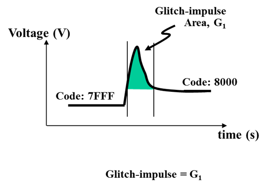
When designing with a digital-to-analog converter (DAC), you expect the output to move from one value to the next monotonically, but real circuits don’t always behave that way. It’s not uncommon to see overshooting or undershooting, quantified as glitch impulse, across certain code ranges. These impulses can appear in one of two forms, shown below in Figure 1.

Figure 1: DAC glitch behaviors
Figure 1a shows a glitch that produces two regions of code transition error, which is common in R-2R precision DACs. Figure 1b shows a single-lobe glitch-impulse, which is more common in string DAC topology. Glitch impulse is quantified as a measure of energy which is commonly specified as nano-Volts-sec (nV-s).
But before we can talk about sources of DAC glitch, we must first define the term “major-carry transition.” A major-carry transition is a single-code transition that causes a most significant bit (MSB) to change because of the lower bits (LSBs) transitioning. Binary code transitions of 0111 to 1000 or 1000 to 0111 are examples of a major-carry transition. Think of it as an inversion of the majority of the switches. This is where glitch-ing is most common.
Two areas of concern are switching synchronization and the switch charge transfer, as multiple switches are simultaneously triggered. For the sake of argument, let’s look at an R2R string DAC that’s designed to rely on switches that are synchronized during code transitions, shown below in Figure 2.

Figure 2: DAC major carry transition
As we all know, there’s no such thing as perfect synchronization, and any variance in the switching will lead to a brief period where all switches are either switched high or low, causing the DAC’s output to error. Recovery occurs and, as a result, a switch charge will create a lobe in the opposite direction, before settling out.
So let’s take a look at the three stages that take place during a major-carry transition and how the DAC output responds, in Figure 3.

Figure 3: DAC output during transition
- The initial stage of the DAC, prior to the code transition. In this example we’re looking at the 3 MSBs representing binary code 011.
- The DAC output enters a major-carry transition that causes, for a short period, all of the R-2R switches to be connected to ground.
- The DAC recovers following a small period of switch charge injection, and the output begins to settle out.
Comparing the output glitch from a major-carry transition versus a non-major-carry transition, illustrated in Figure 4, proves that switching synchronization is the major contributing factor.
X-axis scale is 200ns/div and the Y-axis scale is 50mV/div.

Figure 4: R-2R DAC output glitch
So far, we’ve looked at glitch in an R-2R DAC architecture to explain that switch synchronization is the major contributor. But when you look at the glitch-ing of a string DAC, it is a little different. By design, it taps into different points on a resistor string to produce the output voltage. Without multiple switching, the pulse amplitude is smaller, and often dominated, by digital feedthrough. A comparison of the same major-carry code transition of an R-2R DAC and string DAC topology is shown in Figure 5.

Figure 5: R-2R vs string DAC output glitch
Understanding why glitch-ing occurs can help you decide if your design can live with this short impulse. I’ll talk about some methods to help reduce glitch in the coming weeks.
And if you want to learn more about string and R2R DACs, be sure to check out these previous posts in our DAC Essentials series here on Analog Wire:
- DAC Essentials: String theory on string DACs
- DAC Essentials: The resistor ladder on R-2R DACs
Thanks for reading; I promise my next post will be shorter. :-)