Quantcast
Channel: Analog
Viewing all 585 articles
Browse latest View live

A race against the clock: how to determine the power-up states of clocked devices

$
0
0

Many engineers choose flip-flops, shift registers, or other clocked devices for temporary storage and moving small amounts of data. These clocked devices have one or more clock-input pins, typically designated CLK or CP. A clock edge will determine when a specific function occurs; for example, the data may be clocked to an output, or data may be moved from one pin to another. Device data sheets specify whether this happens on the positive or negative edge, and include a truth table for each part.

Often, these truth tables include up and down arrows indicating the clock status. But what happens in that mysterious state before any clock edge has occurred? Consider the SN74AUP1G80, a five-pin D-type flip-flop. If VCC powers up and there is no valid clock edge, the truth table says that the Ǭ output is equal to Ǭ0.

Not very helpful, is it? Actually, it illustrates a design reality. We don’t know what the output will be before the first valid clock edge. When the device turns on, thresholds on internal transistors in the clocked device can float to indeterminate values, resulting in unpredictable signal levels at Ǭ. Typically, under the same conditions, the part will start up with the same output value, but this can vary across temperature and manufacturing lot to another. Therefore, for these clocked devices, it is imperative to wait until VCC has ramped to an appropriate level and a valid clock edge has passed before reading the output.

If the clock edge on a positive-edge-triggered device rises with VCC, I recommend waiting an extra clock cycle, as the clock threshold changes with VCC and any small amount of noise can cause unwanted clocking.

One clever trick you can use to “beat the clock” is to use devices with clear (CLR) (set all outputs to 0) and preset (PRE) (set all outputs to 1) inputs. Typically, in TI data sheets we designate these pins by some form of PRE, CLR or MR (for master reset). Look at the SN74AUP1G74, for example. The active-low CLR and PRE inputs allow engineers to override the clock! When used, these pins allow you to set the output of the device before CLK, giving you more control over the output bus. 

For more advice on powering clocked devices, review these additional resources:


Extending battery life for IoT applications

$
0
0

As the world constantly evolves to keep everything and everyone connected, wireless sensors are becoming more and more popular in the Internet of Things (IoT) market. Several definitions for the IoT exist, but one simply defines it as keeping up to date with our surroundings by measuring the environment with remote sensors.

Figure 1: IoT system high-level description

Most IoT applications operate in burst mode, where the system is asleep most of the time. Due to this duty-cycled system behavior, the sleep current becomes extremely important in determining how well the system can conserve battery power and extend the device’s lifetime. In recent years, technological improvements have led to a drastic reduction in system sleep current to only a few tens of nanoamperes, but there’s much more potential to drive system power even lower.

A low-power system timer could be especially beneficial for duty-cycled or battery-powered applications like those you’ll find in IoT applications. That’s why TI introduced the TPL5110 and TPL5010 low-power system timers. Normally in such systems, the microcontroller’s internal timer is used to duty-cycle the system; however, even in low-power or sleep mode, the microcontroller (MCU) can still use several microamperes.

Consuming only 35 nA, the new timers can interrupt the system periodically, drastically reducing the overall system standby current during sleep (Figure 2). Such power savings enable the use of significantly smaller batteries, making them applicable for energy-harvesting or wireless-sensor applications. The timers provide selectable timing intervals from 100 ms to 7200 s and are designed for duty-cycled applications.

Figure 2: Theory of operation

The TPL5010 operates by sending a wake-up signal to the MCU during every programmable delay period (Figure 3). When an MCU works in conjunction with the TPL5010, it can operate in an even lower-powered sleep mode by turning off its internal timer. In addition, an integrated watchdog function constantly checks the system’s MCU ensures high reliability. (For more about this watchdog function, check out the datasheet.)

Figure 3: TPL5010 low-power system timer with watchdog function 

The TPL5110, on the other hand, operates by driving an external metal-oxide semiconductor field-effect transistor (MOSFET) to power-gate the system’s supply for even greater power savings. In addition to this normal duty-cycled timing function, the TPL5110 can operate in “one-shot” mode. In one-shot mode, the timer can drive the MOSFET for a single cycle. Coupled with a manual-reset functionality, these two features make the TPL5110 a small and low-cost solution ideal for any simple power-on applications without the need for an MCU.

Figure 4: TPL5110 low-power system timer with MOSFET driver

Let’s take a look at a brief application example.

Figure 5: Typical wireless sensor

In the case of an application where humidity and temperature sensors are being used to monitor the environment, measurements are normally taken once per minute. This means that the duty cycle will be active for approximately 1 s and in off or sleep mode for 59 s. Now normally, an MCU can control the system timing; but if the MCU's sleep current is 120 μA, the system will be burning excess current. With the TPL5110, you are only operating at 35 nA in off mode, which is almost 3,500 times less.

Additional resources:


On Board with Bonnie: ADC noise from the inside out

$
0
0

I must apologize. I am going to approach analog-to-digital converter (ADC) noise from an analog perspective. You may be surprised about this view because this discussion usually focuses on a digital perspective, but the analog outlook does work out quite elegantly.

Delta-sigma ADCs such as the ADS1220 (Figure 1) give you detailed information about generated data converter noise. The units of this noise description, en, are microvolts-rms (µVrms) and microvolts peak-to-peak (µVp-p).

Figure 1: Resistive bridge measurement using the ADS1220 precision ADC

You can think of this noise as a referred-to-input phenomenon, similar to an amplifier (Figure 2). With the amplifier, the units of noise, en, are nanovolts per root hertz (nV/ÖHz). Over a specified bandwidth, the en units are microvolts-rms (µVrms). Another unit of measure for operational amplifier (op amp) noise is microvolts peak-to-peak (µVp-p).

Figure 2: Op amp circuit with a closed-loop gain of –200 V/V

Let’s now look at the referred-to-output noise of a delta-sigma ADC and op amp. Both are closed-loop systems, where the ADC processes the signal with an internal digital filter and the amplifier has an external resistor network. In both cases, the devices send the output-noise signals to the output pin. In the case of the ADC, this would be the DOUT pin. In the case of the amplifier, this would be the VOUT pin (and you are looking for the total noise).

Typical specifications for the delta-sigma ADC’s output noise are effective-number-of-bits (ENOB) and noise-free-bits (NFb). Equations 1 and 2 are generic formulas for these two specifications:

ENOB = log[(2*VREF/GAIN)/( en_uVrms)] / log 2                   (1)

NFb = log[(2*VREF/GAIN)/(en_uVp-p)] / log 2                        (2)

where VREF is the data converter’s applied voltage reference and GAIN is the data converter’s gain, per an internal programmable gain amplifier (PGA).

These specifications are very important if you plan to compare ADC to ADC, but consider the power behind the noise specifications when determining the repeatability of your sensor system.

In Figure 1, the sensitivity of the load cell is 2 m/V and the maximum capacity (FSg) is 100 kg. For this system, the repeatability in grams (REPg) or minimum measurement value is equal to Equation 3:


REPg = en:p-p * FSg / (AVDD * Sensitivity)                 (3)

where AVDD is the voltage across the bridge as well as the ADS1220 positive analog supply.

For this ADC, at a data rate (DR) of 20 SPS, a PGA gain of 64 and in normal mode, FSg is equal to 100,000g and ADS1220µVPP noise is 0.35 µV (per Table 1).

REPg = FSg (1 - en:p-p / (AVDD * sensitivity))

REPg = 0.35 µV * 100 kg / (5 V * 2 mV/V)

REPg = 0.7 gm

Table 1: ADS1220 in µVRMS (µVPP), normal mode

The analog point of view is useful in the oddest places. With load cells and delta-sigma ADCs, you can stretch your imagination into the analog domain and use the specifications to your system’s advantage.

Additional resources:

Don’t procrastinate, isolate! The need for a basic galvanic isolator

$
0
0

Digital galvanic isolation has an important part to play in the world. It does an amazing thing: it protects precarious products from unscheduled electrical blowback like a suit of armor might against an unsuspected ricochet on the battlefield.

In addition to this protection, it also facilitates communication between devices.  Sometimes two devices might be on different ground planes but still need to be in contact with each other.  To illustrate both of these benefits, let’s look at a 3V microcontroller (MCU) that needs to turn on a 100V motor.  

Chances are that the MCU is on a digital ground, and the motor is on an analog ground plane.  If you were to connect the control lines of the motor directly to the MCU, you’d create a ground loop and ground potential difference (GPD) that may inhibit signals from the MCU passing to the motor.  Not to mention the connection alone might fry the MCU, but if for some reason the MCU’s control signals make it through this GPD and turn on the motor; the back electromotive forces (EMF) generated from the motor turning could come back and fry the MCU altogether!   If you designed your system this way, don’t fret… it’s not too late to isolate.  Good things take time, so don’t misinterpret procrastination as laziness; all engineers know that truly it is efficiency. No matter your design it’s never too late to add isolation.

Galvanic isolation comes in multiple formats as well as varying degrees of protection. Another way to look at it would be through the eyes of Goldilocks: one that is “just right” when others seem to be “too hot” or “too cold.” Starting off at the most isolation protection you can get, I'll address reinforced isolation.  You may have heard about TI’s reinforced digital galvanic isolators, announced during the electronica trade fair in Munich.

These devices offer bulletproof ruggedized protection which is called for in some scenarios, such as harsh industrial environments dealing with very noisy signals that can spike up very quickly.  These might be seen as “too hot” in the Goldilocks scenario.  Functional isolation on the other end is the lowest form of isolation, where protection is offered but minimal levels or “too cold,” and basic isolation is in between being not too hot and not too cold in terms of protection, but just right.

Basic galvanic isolation covers you when you need more than “a little” but less than “a lot” of protection in environments where things can get noisy but not apocalyptic. For example, in any major industrial design there is most likely a power block connected to a noisy power supply. Depending on the quality and noise-rejection capability of that power supply (perhaps even inside it), you’d probably want to employ a reinforced isolator, since it could deal with the majority of the challenging electrical interference. What is then cleaned up and passed along to be used by the system itself should be OK to use, but what happens in theory doesn’t always translate in the real world. Thus, you might need a little more isolation in the rest of your system. This protects against runaway power-supply pulses or internally generated spikes from sensors or other industrial equipment like motors, fans, servo controls and protects more delicate microcontrollers or microprocessors or even a more costly field programmable gate array (FPGA) or digital signal processor (DSP).

So don’t procrastinate; isolate!  Find a galvanic digital isolator that’s just right for you. In fact, TI has a new line of basic digital galvanic isolators. Compared to our previous generation, these capacitive-based digital isolators offer:

  • A 20% higher UL 1577 isolation rating of 3.0kVRMS.
  • 50% higher DIN V VDE V 0884-10 maximum-surge voltage rating of 6kVPEAK.
  • 80% lower active power.

If all of your galvanic digital isolators have been “too hot” and “too cold,” perhaps you should check out TI’s line of “just right” basic digital isolators and keep your design comfortable and covered.

Additional resources:

If you don’t see what you’re looking for, try searching for asking a question in our TI E2E™ Community Industrial Interface forum.

JESD204B: Serial link quality tradeoffs and tools for optimization

$
0
0

One of the most important goals in a JESD204B system design is achieving good signal quality in the serial data link. The signal quality is determined by the circuit board dielectrics, the quality of the signal routing, any connectors in the signal path, and the TX and RX device circuitry. In this post, I’ll focus on the effect of the dielectric materials and RX and TX device features related to optimizing signal quality.

JESD204B serial links operate at very high bit rates, currently up to 12.5Gbps. At these high data rates, standard FR4-type materials cause significant loss of the higher-frequency components of the signal. The amount of loss depends on the exact material used, the link data rate and the length of the TX/RX link.

Figure 1 shows signal loss versus frequency for a typical FR4-type material (Isola 370HR) compared with that of a high-performance, radio frequency (RF)-oriented material (Panasonic Megtron 6).

Figure 1: Printed circuit board (PCB) insertion loss

Higher-loss materials are not bad per se, but the loss must be understood and planned for as part of the system and subsystem design. You should also consider these loss characteristics when planning the analog signal and clock portions of the design, in addition to that of the serial data link. You will need to evaluate the needs of the overall system when planning the PCB material choices and board stackup. It may be possible to use an entirely FR4-type board, a board with high-frequency dielectrics on selected layers or on all layers as needed. Let’s review some of the design considerations.

For the serial data link, the receiving device will operate correctly with acceptable bit error rates as long as the signal at the receiver inputs meet the JESD204B receiver eye-mask specifications. (See sections 4.4, 4.5 and 4.6 of the JESD204B.01 standard document). If the losses in the data link reduce the high-frequency content in the signal too much, the received eye will begin to close and fail the receiver eye-mask.

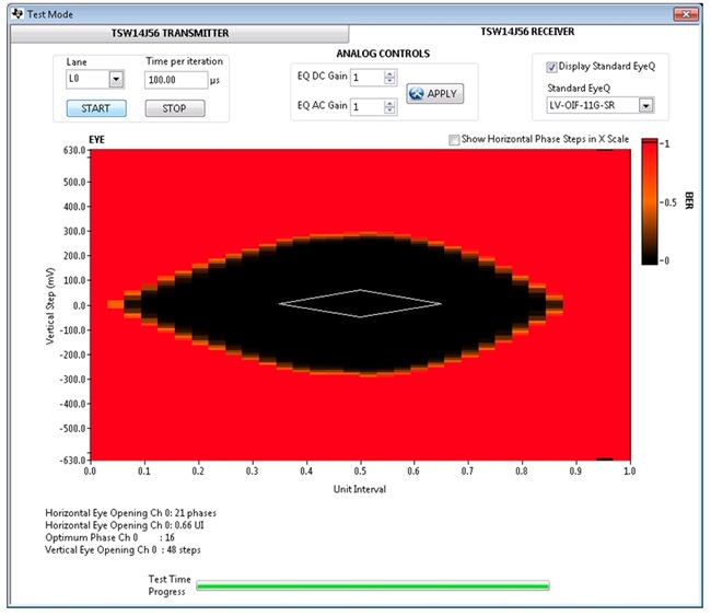
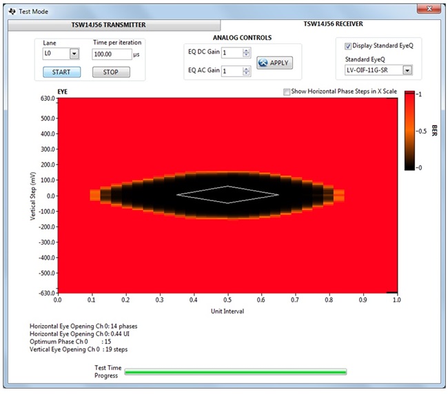
Figure 2 is an example of an open eye diagram acquired using the ADC12J4000 evaluation module (EVM) and TSW14J56EVM along with High Speed Data Converter Pro Software.

Figure 2: ADC12J4000EVM connected to TSW14J56EVM, both using high-performance materials, analog-to-digital converter (ADC) at 4GSPS in decimate-by-4 double-data-rate (DDR) P54 mode (data at 10Gbps) and a default pre-emphasis setting of 4d

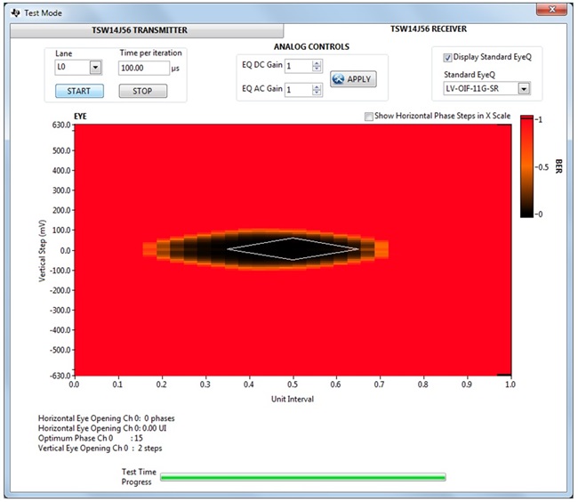
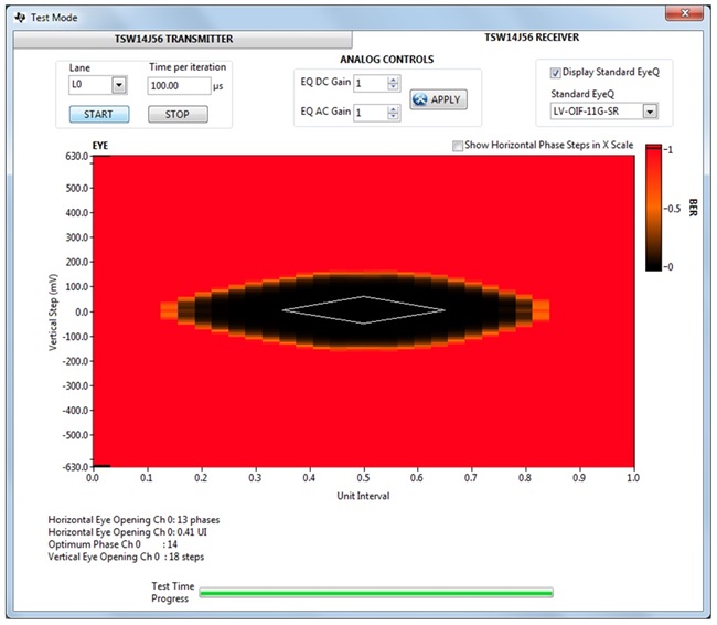
Figures 3 and 4 show the same baseline setup as in the open eye example, but with two different extender boards connected between the baseline EVMs. These extenders were added to evaluate the effects of longer links and lossier materials. Figure 3 is with a 16-inch trace extender board using Rogers RO4350B, another high-performance material. Figure 4 is with a 16-inch extender board using Isola 370HR FR4-type higher-loss material.

Figure 3: Baseline hardware plus 16-inch RO4350B extender board, 4GSPS in decimate-by-4 DDR P54 mode (10Gbps) and default pre-emphasis setting of 4d

Even with high-performance materials, long link distances attenuate the high-frequency signal components and begin to close the signal eye.

Figure 4: Baseline hardware plus 16-inch 370HR extender board, 4GSPS in decimate-by-4 DDR P54 mode (10Gbps) and default pre-emphasis setting of 4d

With a long link using the lower-cost material, the eye quality is severely degraded.

To restore the eye quality at the receiver, you must either select a lower-loss board dielectric or alternatively add some compensation at the serial TX/RX.

Many JESD204B TX/RX devices (ADCs, field-programmable gate arrays [FPGAs]) and digital-to-analog converters [DACs]) incorporate signal-quality compensation circuitry to mitigate the effects of high-frequency signal loss. ADCs will include pre-emphasis (boosting the high-frequency content) or de-emphasis (reducing the low-frequency content) features. On the receive side of the link, DACs and FPGAs may include equalization (adjust gain at different frequencies to optimize the equalizer output eye quality).

Using the TX pre- or de-emphasis feature can allow a system to operate with acceptable receive performance even with lower-cost FR4-type transmission media or longer-than-normal link distances. In these situations, the emphasis features are adjusted until the receive eye meets the specifications with some margin, but without excessive overshoot.

With the same extenders, the ADC12J4000 TX pre-emphasis settings were increased to optimize the data eye at the receiver. Figures 5 and 6 show the eye diagrams after optimizing the pre-emphasis settings for the high performance and FR4 type extenders. A significantly higher pre-emphasis setting is necessary to compensate for the additional loss of the lower-cost material.

Figure 5: Baseline hardware (ADC12J4000EVM + TSW14J56EVM) plus 16-inch RO4350B extender board, 4GSPS in decimate-by-4 DDR P54 mode (10Gbps) and pre-emphasis setting of 7d


Figure 6: Baseline hardware (ADC12J4000EVM + TSW14J56EVM) plus 16-inch 370HR extender board, 4GSPS in decimate-by-4 DDR P54 mode (10Gbps) and pre-emphasis setting of 15d

As I mentioned earlier, the input-signal and clock-signal paths can also drive the requirements of the board materials and stackup. Even if emphasis or equalization features permit link operation using lower-cost board materials, you may still need some higher-frequency layers to minimize signal-quality impacts for the analog or clock signals in a high-frequency design. You must consider all of these factors when selecting the board dielectric materials and planning the board stackup. Once you’ve made those choices you can design, build and test the system. In the testing and debugging phase of the design, you can adjust the TX pre- or de-emphasis settings and RX equalization settings to provide a reliable data link.

Additional resources:

The future of data converter interfaces

$
0
0

I’m a very direct individual, and when I think of data-conversion technology, I quickly categorize it into buckets:

  • Precision:  Typically less than 1 Msps with a high dynamic range (+20 bits).
  • General purpose:  Anywhere from 1 Msps to 20 Msps with a moderate dynamic range (12-16 bits).
  • High speed:   20 Msps to 1 Gsps with a good dynamic range (8-14 bits).
  • Ultra-high speed:  1 Gsps and above.

For lower-speed precision and general-purpose data converters, serial peripheral interface (SPI), I2C or parallel interfaces are more than enough to handle the data rate. But what happens when you can now integrate four or eight digital-to-analog converters (DACs) or analog-to-digital converters (ADCs) that each require 100+ Msps per channel? The digital information overwhelms the standard interfaces.

The solution for multiple data converters at or above 100 Msps has been to use either parallel double-data-rate (DDR) low-voltage differential signaling (LVDS) or serialized LVDS. At first, serializing the LVDS seems logical, but LVDS is limited in performance. When serializing large numbers of moderately fast data converters or small numbers (one to two) of ultra-high-speed data converters, lane speeds will exceed 3 Gbps – this is pushing the limits of LVDS technology. In addition, serialized LVDS requires a clock line to synchronize each lane, while the transmission lines still require matching to prevent skew and jitter from affecting bit error rate (BER).

The first true solution to the steady progression of ever-faster analog data converters is the JEDEC standard JESD204. In the latest revision, B, the interface has moved from LVDS to current-mode logic (CML), which is designed for speeds in excess of 10 Gbps. Additionally, the clock is now embedded into the stream, allowing independent clock and data recovery per lane. The standard also introduced scrambling and 8b/10b encoding to both minimize electromagnetic interference (EMI) and improve data integrity. This migration greatly reduces the number of interconnects required between the data converter and processor or field-programmable gate array (FPGA).

For example, an ADC12D1600 running in dual-edge-sampling (DES) mode provides a sample rate of 3.2 Gsps, which requires 50 electrically matched LVDS transmission lines, whereas the ADC12J4000 only requires eight CML transmission lines (which do not need to be electrically matched). The skew is adjusted by an elastic buffer inside the receiver’s JESD204B interface. This also benefits the package, which shrinks from a 292-pin ball-grid array (BGA) (ADC12D1600) package to a 68-pin very thin quad flat no-lead (VQFN) package (ADC12J4000) that is only 10 mm x 10 mm. So both performance and density benefit from this interface technology (Table 1).

Table 1: Comparison of two similar gigasample ADCs, one with a parallel LVDS interface and the other with JESD204B

However, there are issues with this interface technology: latency and signal integrity. One benefit of parallel LVDS is that the delay between the time the sample is acquired from the ADC (or presented to the DAC) is extremely short. In the case of a gigasample ADC, it is a matter of converting a thermometer code to either 2’s compliment or binary – a straightforward digital single-clock cycle function and the data is immediately available at the outputs. In the case of the JESD204B, the data is scrambled, 8b/10b encoded and finally serialized, which all then needs to be reversed at the receiver. This adds considerable latency in the transmission of the data, even with lane speeds of 12.5 Gbps.

Then there’s signal integrity. CML lanes running at 12.5 Gbps on FR4 can be challenging. Beyond the forward-loss factor of the board material, there can be impairments such as connectors and vias that will add to the overall jitter budget of the interface. For longer transmission lines, a buffer/equalizer may be required such as the DS125BR800A, which can provide receive equalization as well as increased drive including de-emphasis to improve the BER of up to eight lanes – a major factor considering that there is no forward-error correction in the JESD204B standard.

So what does the future hold? In much the same fashion that data centers require faster interconnects, so will high-density or ultra-high-speed data converters. The current JEDEC standard specifies CML transmission lines that can run up to 12.5 Gbps. The next-level standard will take that to 16 Gbps or beyond – possibly 25 Gbps – driving the need for careful signal-integrity management and possibly the introduction of more exotic board materials such as Megtron 7. It is the price of going faster, but the benefits of high-speed serialization coupled with standardized protocols outweigh the issues. Till next time …

JESD204B resources:


How to protect USB host ports with ESD current-limit protection devices

$
0
0

One of the hottest topics regarding interface technology today is the universal serial bus (USB) Type-C connector, popular for its reversibility, higher data transfer, power delivery and additional protocols. While there is much excitement over the new standard, the reality is that the USB Type-A connector is still prominent and is being designed into end equipment today. When designing for USB host ports, you should consider two major areas of protection: overcurrent protection and electrostatic discharge (ESD) protection.

Overcurrent protection

Per section 7.2.1.2.1 of the USB 2.0 specification, “All host and self-powered hubs must implement overcurrent protection for safety reasons.” You can accomplish this by using a fuse or current-limit switch. Moreover, a current-limit switch is the preferred solution over a fuse because it allows you to allocate less power per port during design. In a transient event, the load switch limits the output current to a safe level by operating in constant current mode. A fuse will allow the current to rise above the maximum current level until it shuts off. Choosing a current-limit switch allows you to select a smaller DC/DC converter and inductor because the switch more accurately limits the current during an overcurrent event. The current-limit switch also allows for decreased Vdroop in the 5V Vbus during transients versus a fuse implementation.

ESD protection

When designing USB ports, you should be aware of the high risk for ESD strikes and consider using ESD protection to prevent damage. For example, USB controllers and transceivers often handle ESD ratings based on the human body model. This rating is the oldest and most commonly used to detect ESD sensitivity. The HBM rating is intended for chip-level ESD protection and does not guarantee that the system will be protected from higher level ESD strikes. The International Electrotechnical Commission (IEC) 61000-4-2 standard tests for higher levels of ESD energy when compared to the HBM rating, as shown in Figure 1. For system-level protection, consider selecting the more robust IEC 61000-4-2 standard and using a transient voltage suppressor (TVS) diode.

In USB 2.0 applications, system-level ESD protection should be considered for VBUS and the data lines. VBUS requires a large capacitor for handling power transients like hot-plugging, and therefore can pass IEC 61000-4-2 by means of the capacitor. However, the data lines require a different approach. The high-speed lines operate at a maximum data rate of 480 Mbps, which means a large capacitor cannot be added to protect from ESD. You will need a low-capacitance TVS diode in order to decrease the effect on signal integrity.

Figure 1: ESD test comparison

Complete solution

Traditionally, multiple devices met the protection requirements for a USB host: a current-limited load switch for Vbus plus one or more ESD protection devices for the data pins. The TPD3S014 combines a current-limit switch and two channels of ESD protection to make a single-chip USB host-port solution as shown in Figure 2. The TPD3S014 and TPD3S044 allow 0.5A and 1.5A of continuous current, respectively, in a space-saving 2.9 mm by 2.8 mm DBV package.

The current limits in this family feature reverse-current blocking and are Underwriters’ Laboratories (UL)-recognized components (UL2367). They also provide IEC 61000-4-2 (Level 4) ESD protection for the data pins. These devices simplify your designs by reducing the number of devices and shrinking the overall footprint of the printed circuit board (PCB) to ensure optimal USB host-port protection.

Figure 2: USB host-port protection solution

Additional resources:

RF Sampling: The new architecture on the block

$
0
0

** This is the first post in a new RF-sampling blog series that’ll appear monthly on Analog Wire **

The need for bandwidth is insatiable. We want more gaming, more video streaming and more social-media interactions on our smartphones. Plus, there are more people accessing the networks than ever before. All of this translates to a network that must use more bandwidth to support the data and capacity requirements we demand. 

Figure 1 illustrates a traditional receiver architecture for supporting high-bandwidth signals. The mixer stage converts the signal from the radiofrequency (RF) spectrum to a fixed intermediate frequency (IF). From there, a quadrature demodulator converts the signal down to complex baseband (BB), where it is sampled by a two-channel analog-to-digital converter (ADC) and passed along to the digital processor.

The Nyquist sampling theorem dictates that the sampling frequency must be at least twice that of the signal bandwidth; but in practice, it needs to be even higher.

When the data converter sampling rate is the limiting agent, it is imperative to use all of the tricks available to reduce that bandwidth. The demodulator splits the signal into two quadrature paths, each with half the bandwidth of the original signal. Even with that trick, it is difficult to find a data converter with sufficient sampling-rate capability and dynamic range to capture the wideband signals needed for high-end communication equipment…until now.

Figure 1: Traditional super-heterodyne receiver architecture for wideband signals

New higher-sampling-rate data converters with sampling rates up to 4GSPS and beyond can directly sample the large signal bandwidths. Further, the devices can operate directly in the RF band. This opens up a new architecture option, as shown in Figure 2. The RF sampling receiver architecture eliminates the RF mixer stage and its associated local oscillator (LO) synthesizer. It eliminates the quadrature demodulator and associated BB circuitry and LO synthesizer and replaces the two-channel ADC with a single RF-sampling ADC. The signal path has been tremendously simplified with the introduction of RF sampling ADCs.

Figure 2: RF-sampling receiver architecture

The RF-sampling architecture opens up new possibilities for system designers – most notably higher bandwidth and more flexibility. RF-sampling data converters can support higher bandwidths, which enables higher data transfer rates. The architecture also provides more flexibility. The desired signal can be easily captured anywhere in the RF band – without the need for analog tuning. In fact, the exact location of the signal does not even need to be known. The entire spectrum can be captured and then the specific signal can be extracted digitally in the processor. Further, reducing component count improves power-dissipation and reduces cost.

RF-sampling data converters, like the 4-GSPS ADC12J4000, enable higher-density systems that take advantage of beam-forming antennas or massive antenna arrays where channel count increases. The architecture is paving the way for more flexible, cost-effective solutions today and new higher data rate and capacity systems for next-generation systems.

I hope you’ll come back next month for my post on why you should adopt RF sampling.

Additional resources:


Trimmed or chopped: How do you like your op amp?

$
0
0

Depending on the application you’re working on, smaller offset voltages do not always mean higher precision or better DC performance. First, you need to determine the most dominant source of error. If indeed it is the input offset voltage then chopper-stabilized (zero-drift) operational amplifiers (op amps) come in handy. They give you the lowest input offset voltage … and yes, the lowest drift … and yes, practically no 1/f noise. They are extremely useful in high-gain circuits and wider temperature range applications.

In applications with a narrow temperature range such as medical instrumentation, the very low offset drift may not buy you a lot – at least not when compared to the input bias current of your amplifier coupled with the source impedance. This could be a major concern with a zero-drift device, as their input bias current can be orders of magnitude higher than a standard complementary metal-oxide semiconductor (CMOS) or field-effect transistor (FET) input device.

For narrow temperature range applications, you’re better off using a well-trimmed device such as the OPA376 instead of the OPA333, for example. The difference in the initial offset voltage is 15µV, but the difference in input bias current is 190pA! With a source impedance of 1MΩ, your error is 190µV, a much larger value than the initial value for input offset voltage of 10uV of the OPA333.

Another advantage of non-zero-drift op amps is their ubiquitous use in precision measurements. Chopper-stabilized amplifiers can have limitations depending on the application and circuit configuration.

If you’re considering a zero-drift device to use as a buffer, you may want to consider adding a simple filter at its output to avoid the glitches (chopping) that typically reside in the unity-gain bandwidth of the op amp.

For advice on more complex filters, check out this blog on active filtering.

Additional resources:

4K video transport made easy

$
0
0

The National Association of Broadcasters (NAB) show is just a few days away; the broadcast video world will take over Las Vegas to showcase their latest innovations April 13-16. Over the years, this market has evolved from standard definition (SD) (SMPTE-259M) to high definition (HD) (SMPTE-292M) to 3G (SMPTE-424M). Fueled by the four-times-higher resolution, some content providers have already begun producing 4K content.

While the complete deployment of 4K could be as slow as the SD-to-HD transition, the transition is inevitable. 4K adoption will speed up when the cost premium of 4K content creation, transport and display becomes acceptable.  Consumers then would be able to enjoy streaming 4K videos with higher clarity. In order to support ultra-high-definition 4K, semiconductor manufacturers need to deliver serial digital interface (SDI) devices capable of 12G performance to enable transmission over a single link.

A single link for SDI has traditionally been synonymous with coax cables. But recently, the video market has considered the use of the Internet protocol (IP) infrastructure (10 gigabit Ethernet) to facilitate video transmission (SMPTE 2022-5/6). As the IP infrastructure is available for transmission up to 100Gbps, it makes complete sense to tap into existing resources for video transport. Being a lower cost and widely used protocol makes IP attractive for the 4K transition. Depending on the system’s reach requirements, SDI or IP or both could be used. We are definitely looking forward to the dialogue and announcements tied to 4K/ultra-high-resolution (UHD) transport over SDI and IP at NAB this year.

Our latest innovation for broadcast video makes it easy for equipment manufacturers to take either approach for their 4K transmission link: IP or SDI.  The LMH1218 is the industry’s first 12G cable driver to support both SDI- and IP-based 4K video transmission. The LMH1218 gives you the flexibility to design video-infrastructure equipment for either the SDI or IPformats using a single device. In addition, the device supports coax cable for short-haul networks and optical media for long-haul communication.

Jitter performance of the link is a key factor in quality of video transmission, making the difference for end users between a smoothly streaming video and annoying breaks or flickering in the transmission.  This jitter becomes even more critical at higher date-rates given the media bandwidth limitations, requiring the signal to be reclocked before transmission. Featuring an integrated reclocker, the LMH1218 eliminates the need for an external reclocker, thereby simplifying system design. These features, packed in a 4mm x 4mm quad flat no-lead (QFN) package, should put you at ease when deciding between the protocol (SDI or IP) or media (coax or optical).

To learn more about the capabilities of this device and to see a demonstration of the LMH1218, stop by TI’s booth, N8519, at the NAB Show April 13-16. If you happen to miss the show, you can learn more about the LMH1218 by reading its data sheet.

Additional resources:

Inductive sensing: Meet the new multichannel LDCs

$
0
0

If you have been reading my blog series on how to design inductive sensing with the LDC1000 inductance-to-digital converter since we released it , you know how excited I am about the many uses and design opportunities. But until now, design could have been a bit complicated when your system required multiple inductive sensors. That’s why I’m now excited to share that TI has expanded our inductive sensing portfolio to include four new 3.3V I2C multichannel devices: the LDC1312, LDC1314, LDC1612 and LDC1614 (see Figure 1).

 Figure 1: TI’s new inductive sensing solutions


The LDC1312 and LDC1314 are 12-bit inductance-to-digital converters (LDCs), which can be used for applications such as rotational knobs, keypads or flow meters. The LDC1612 and LDC1614 are 28-bit LDCs, which can be used in high-precision applications such as linear encoders or strain gauges.

 Here are some reasons to consider a new LDC device for your next design.

 Multichannel operation

With the dual-channel LDC1312 and LDC1612 devices and the quad-channel LDC1314 and LDC1614 devices, system design can become much simpler while also improving cost effectiveness. The inherent channel matching from using a multichannel LDC improves system performance in high-precision designs that either employ differential measurements, or use one coil as a reference to reduce the effect of temperature, mechanical tolerances or other system variables.

 Sensitivity

The maximum sensing distance changes with coil diameter. As with the LDC1000, the LDC1312 and LDC1314 operate best if the maximum target distance is kept within 50% of the coil diameter. However, the high-resolution of the LDC1612 and LDC1614 can effectively sense targets as far as two coil diameters away from the sensor.

 Power consumption

We significantly improved power consumption of the new LDC family to benefit battery-operated applications. Lowering the supply voltage from 5.0V to 3.3V allowed us to drop power consumption in active mode by 20%, from 8.5 mW to 6.6 mW. Standby-mode power consumption dropped by 91%, from 1.25 mW to 0.11 mW. Additionally, the new LDC family features a pin for shutdown mode, during which the device consumes only 0.2 µA.

 In low-sample-rate battery-operated applications, the sleep mode and shutdown mode functions can be used to cycle the LDC. The LDC turns on to perform the conversion and then retunrs to one of the low-power modes. The Inductive Sensing Design Calculator Tool contains a power-consumption estimator for this purpose.

 Start designing

Each of the four multichannel devices has a new evaluation module (EVM) (Figure 2), which is available now. Together with our new multichannel EVM software, you can get started with the new features of our inductance-to-digital converters within minutes. You can also check out the EVM and GUI quick-start videos.

Figure 2: LDC1312/LDC1612 EVM


In upcoming posts, I will explain how to configure a multichannel system and explore the possibilities that the increased sensing range of the LDC1612 and LDC1614 offer.


Additional resources:

Make a turbo amp your designated driver

$
0
0

If you’re using a high-resolution (16- and 18-bit) successive-approximation-register (SAR) analog-to-digital converter (ADC) in your design, you’ve probably faced the challenge of finding the best possible amplifier to drive it.

One of the most common challenges is maintaining a low noise floor without having a horrendous power budget in the analog front-end. In other words, the only way to get a low noise floor is to pump large amounts of current into the operational amplifier (op amp). Integrated circuit (IC) designers may also need to use bulky transistors in the input topology, which limits their ability to use a small footprint and adds substantial cost due to the die-size increase.

What if you could have a scalable amplifier in the front-end? I’m talking about a device that combines a high-power mode, a low noise floor (2.5nV/rtHz), a superb settling time (200ns for 0.0015% off a 4V step) and a low-power mode such that the op amp only draws about 0.25mA of quiescent current. This would be a “turbo amp” like the OPA625.

The OPA625 can be used in high-power mode while the ADC is in acquisition mode, thereby enabling enough bandwidth, slew rate and current for its output to settle quickly, as well as a noise floor low enough to maintain the optimal system effective number of bits.

The scalability, low offset voltage and low drift aspects of such an op amp offer a clear advantage over its high-speed counterparts. Its low distortion also helps maintain signal integrity.

With a wide bandwidth and low quiescent current, it offers high performance in AC and DC wise.

Because the OPA625 is built on a complementary metal-oxide semiconductor (CMOS) process, it is versatile and can be used in a broad range of applications. The combination of low voltage and current noise makes it beneficial for interfacing high-impedance sensors, such as piezoelectric and passive infrared (PIR).

So the next time you’re looking to keep your noise under control, give the OPA625 a shot, and get your circuit to quiet down without burning holes in your printed circuit board (PCB).

What application would you use this turbo amp for?

Related technical resources:

An industrial strength education

$
0
0

When looking for answers to questions these days, it’s almost instinctive to use the Internet, often on a portable device. In fact, you are probably reading this post on a battery-operated device, and the only wire you need is for nightly charging (and maybe not even that anymore, thanks to wireless charging).

I also venture to guess that your device is more powerful than all of your childhood computers combined. The Internet in the air! Computing power that used to take up rooms at universities now fits comfortably in your pocket at gigabit-per-second speeds. Though thanks to Parkinson’s Law, where data expands to fill space allotted for it, we will still find ourselves feeling frustrated that it takes “forever” to download a page.

 How do engineers manage to make these technology miracles? Discipline, dedication and a thirst to solve problems are common factors. Engineers also love to learn, through personal and empirical experiences as well as in the classroom.


But what defines a classroom today? The Internet has fundamentally changed how we can learn, effectively leveling the playing field. If innovative thinkers can flip the classroom, then why can’t we flip the engineering classroom? Learning doesn’t have to occur only in the traditional formats; we can learn anywhere with the advancements of technology, including at home, on our commute, on a break from work. Some concepts might not be possible to crack without a full hands-on experience, but you need to lay that foundation first and then build on it.

 Texas Instruments continues to enable this on demand learning. Recently we launched a brand new revamped training portal where you can peruse videos on the latest in topics, spanning from power design, to op amp integration, and multiple topics in between; videos from our engineers to you. If your preferred medium for education is through reading then we have you covered as well. Our interface team is now blogging here on Analog Wire and TI’s new blog dedicated to the industrial market, aptly named Industrial Strength. This new blog includes posts on a range of industrial electronics trends, tools, tips and tricks with deep system-level knowledge. To aid industrial system designers who may have never got specifically interface-oriented technology education in school, TI’s industrial interface engineers will teach some great lessons on current topics. We started with the foundation for industrial interfaces, the RS-485 and CAN bus interfaces.

 To learn more about these interfaces, see the introductory posts below and follow the Industrial Strength blog for more on industrial systems designs and solutions. And watch for posts on these and other interfaces here on Analog Wire as well.

Inductive sensing: How to configure a multichannel LDC system - part 1

$
0
0

Last week, I introduced the latest addition to our inductance-to-digital converter (LDC) portfolio. We released four multichannel LDCs: the LDC1312 and LDC1612, which feature two matched channels; and the LDC1314 and LDC1614, which have four matched channels. In this post, the first in a series, I will explain how to configure them in a multichannel system.

 Benefits

There are several benefits to multichannel designs:

  • Systems that require multiple sensors can now use a single IC, as shown in Figure 1. This results in a lower system cost and greatly simplifies system design because sensors can be placed remotely from the LDC.
  • The individual channels are well matched in terms of parasitics and sensor drive. These well-matched channels can be used for high-precision differential designs, such as the differential linear position sensing shown in Figure 2. Alternatively, one channel can be used as a reference coil that has no target, or a target at a fixed position. The reference-coil channel can be used to set a threshold, compensate for temperature variation, or determine target distance in a lateral or rotational position-sensing system.
  • The reduced system overhead of a multichannel architecture also reduces power consumption.

Figure 1: The new multichannel core simplifies systems with multiple sensors


Figure 2: A multichannel core improves performance in high-precision differential designs

 Channel selection

The LDC has two modes of operation:

  1. Single-channel (continuous) mode: In this mode, the LDC activates the connected sensor and then continuously converts on the selected channel. To put the device into this mode, you would set the following registers:
    1. Put the LDC into single-channel mode by setting AUTOSCAN_EN = 0 (register 0x1B, bit [15]). Note that setting this mode results in RR_SEQUENCE (register 0x1B, bit [14:13]) having no effect.
    2. ACTIVE_CHAN (register 0x1A, bit [15:14]) selects the active channel. Set this value to the desired channel (e.g., 00 will select channel 0).

Keep in mind that the high-current sensor-drive feature (HIGH_CURRENT_DRV, register 0x1A: bit [6]) is only available in single-channel mode for channel 0.

  1. Multichannel (sequential) mode: In this mode, the LDC switches between the selected channels in a round-robin fashion. To configure the device in this mode, set the following registers:
    1. AUTOSCAN_EN = 1 (register 0x1B, bit [15]) to set multichannel mode. When this is set, ACTIVE_CHAN (register 0x1A, bit [15:14]) has no effect.
    2. RR_SEQUENCE = 00 (register 0x1B, bit [14:13]) selects conversion on channels 0 and 1. On the four-channel LDC1314 and LDC1614, option 01 enables three channels (channels 0-2) and option 10 enables all four channels (channels 0-3).

 The multichannel devices include an internal filter to reduce the sensitivity to sensor noise. Set the DEGLITCH setting (register 0x1B, bit [2:0]) appropriately. This setting is common for all selected channels. In some applications, different sensor designs may be used for different channels. Therefore, it is important to choose the lowest DEGLITCH bandwidth setting that is still above the highest-frequency channel.

In this first installment, I’ve explained how to configure LDCs in multichannel mode. If you are using the LDC1312, LDC1314, LDC1612 or LDC1614 in a multichannel system, be sure to check out the next installment in this series, when I’ll explain the timing of these multichannel systems.

 Additional resources

Differential pairs: what you really need to know

$
0
0

The demand for speed is ever increasing, and transmission rates are doubling every few years. This trend is seen in many modern communications systems such as PCIe in computing, SAS and SATA in storage, and Gigabit Ethernet in cloud computing. This information revolution presents huge challenges in delivering data through transmission media, which continue to rely on copper wires and serial bit-stream transfers with a symbol rate >25Gbps and a throughput rate >100Gbps in a data link.

 These serial data transmission designs use differential signaling to deliver data through a pair of copper wires called a differential pair. The complementary signals in the A-wire and B-wire are high-speed pulses of equal amplitude but opposite in phase. Many circuit technologies are used in differential signaling: low-voltage differential signaling (LVDS), current mode logic (CML) and positive emitter-current logic (PECL) are a few examples.

 Delivering a perfect serial bit-stream

 The serial bit-stream is a pair of differential signals propagated through a differential pair. As shown in figure 1, the differential signals are expected to arrive at the same time so that they retain the properties of a differential signal (with equal amplitude, opposite in phase) at the receiving end. A receiver is used to restore the signal fidelity, then sample and recover the data correctly, achieving error-free data transfer.


Figure 1: Electrical properties for a perfect differential pair

 Requirements for a differential pair

 Implementing a well-designed differential pair is a key factor in successful data transmissions at high speeds. Depending on the application, the differential pair can be a pair of printed circuit board (PCB) traces, a pair of twisted-pair copper wires or a pair of parallel wires sharing a dielectric and shielding (usually called twin-axial cable). In this series, I’ll discuss the characteristics of differential pairs, as well as the design challenges and solutions for high-speed data transmission.

 For this first installment, let’s examine the main requirements for a differential pair:

  • Both the A-wire and B-wire need to maintain fairly constant and equal characteristic impedance, commonly called odd-mode impedance, when both wires are excited differentially.
  • The differential signals should arrive at the destination while preserving the differential signal’s properties: approximately equal amplitude and opposite in phase.
    • The insertion loss of each wire should be approximately equal.
    • The propagation delay of each wire should be approximately equal.

 In summary, we are looking for equal and fairly constant odd-mode impedance, minimizing the impedance fluctuation along the length of the differential pair from its source to destination. We are looking for delay matching and insertion loss matching between the A- and B-wires. In addition, we need to make sure the insertion loss is not excessive so that the receiver can recover the data correctly.

To satisfy the above requirements, the A- and B-wires should maintain a high degree of symmetry in their physical layout. The transmitter and receiver should also be highly symmetric in their A- and B-wire circuitry so that they present equal electrical loadings to the A- and B-wires.

Designing differential pairs to minimize distortion

In an ideal world, differential pairs are perfectly symmetrical, have unlimited bandwidth and offer complete isolation from adjacent signals. In the real world, differential signals propagate through integrated circuit (IC) packages, external components, different PCB structures, connectors and cabling subsystems. Implementing a perfectly symmetrical differential pair is a big challenge. In future posts, I’ll discuss differential pair design trade-offs and mitigation techniques to minimize distortions to transmitted signals.

Texas Instruments has a rich portfolio of high-speed signal-conditioning ICs, such as retimers and redrivers. They ease the challenge in mitigating imperfections and high insertion loss from all styles of differential pairs, enabling reliable data communication and extending transmission distance for modern systems.

 Find out more about TI’s LVDS/MLVDS/ECL/CML and signal-conditioning redrivers and retimers. I hope you’ll read the rest of my series on differential pairs.

Additional resources


High-current amplifier applications made smaller

$
0
0

Often, when defining a new device to meet rigorous automotive standards, our teams see other systems that require the same capabilities, and we’ll design the device to cross all these applications. This is what happened when our team was developing the new ALM2402, a dual high-current operational amplifier (op amp) designed for automotive applications.

While defining the ALM2402, we realized that many automotive and industrial systems require an op amp that can drive high-current capacitive or inductive loads.

In the past, designers have often been required to solve this need with discrete components. To design a simple high-current amplifier with discrete components, you need an amplifier, bipolar junction transistors (BJTs) and diodes. An example of this is shown in Figure 1, which is typically used in a motor drive application. This implementation drives the excitation coil of a resolver, which is used to measure degrees of motor shaft rotation. You can find amplifier designs like driving inductive loads in many automotive and industrial applications. This typical solution creates challenges for the designer around board space and biasing of the output transistor.

Adding to the space challenge of the discrete implementation is the need to provide additional circuitry for overcurrent protection. Without overcurrent protection, the system is “dumb.” It will keep burning power without any protection.


Figure 1: Discrete implementation of driving an excitation coil

 In contrast, let’s look at the ALM2402 implementation for driving an excitation coil, shown in Figure 2. Simple, right? No biasing of the external transistor is required, and the ALM2402 can drive up to 400mA through each channel. The circuit is small, housed in a 3-mm x 3-mm DRR package, which allows designers to minimize their overall solution size.

Figure 2: Excitation coil drive using the ALM2402-Q1

Protection is a critical requirement in high-current driving applications, and the ALM2402 integrates several system protection features, including the following:

  • Integrated overcurrent protection
  • Output short to battery if a series diode is connected from the battery to the supply pin of the device. Over-temperature protection shuts down the device if there is an error in layout or a higher-than-specified ambient temperature in the system.

In addition, the device’s flag pin is a handy feature that serves several purposes. The flag pin goes low when an over-temperature event occurs, allowing users to design a feedback mechanism to shut down the system. These can also externally pull down the flag pin to shut down the op amp, which puts it in sleep mode to consume very low current. This feature is useful for battery applications where power consumption is of utmost importance.

Being a high-current operational amplifier, the ALM2402 could be useful for many applications, in addition to motor drives and LED-driving applications. In future posts, I will discuss additional applications that can be implemented using ALM2402.

Additional resources:

Inductive sensing: How to configure a multichannel LDC system - part 2

$
0
0

In my previous post, I explained the benefits and configuration of a multichannel inductive-sensing system with the latest expansion to TI’s inductance-to-digital converter (LDC) portfolio. In this post, I’ll explain how to calculate the timing characteristics of single- and multichannel LDC systems.

Similar to the LDC1000, the new multichannel LDCs have a data-ready signal (DRDY) that can detect when a new data sample is available. Additionally, the timing of the multichannel LDCs is fully deterministic; therefore, it is possible to calculate when a data sample is ready without having to poll the DRDY signal or use the interrupt pin.

The scope plots in Figures 1 and 2 show single-ended measurements of the sensor-input pin in single- and multichannel mode, respectively. In this example, the LDC has been configured with a relatively short conversion time of 128 FREF cycles (CHn_RCOUNT = 0x08), which allows high sample rates at the cost of lower measurement precision.


  Figure 1: Single-channel configuration timing (single-ended measurement on IN0A: yellow and IN1A: cyan)


Figure 2: Dual-channel configuration timing (single-ended measurement on IN0A: yellow and IN1A: cyan)

 Timing of the LDCs is deterministic and can be broken down into:

  • Wake-up time. This is the time it takes to wake up the device from shutdown mode to sleep mode.
  • Wake-up from sleep time. This is the time that the device needs to change from sleep mode to active mode.
  • Sensor-activation time. Sensor-activation time is configured for each channel individually in the SETTLECOUNT_CHn registers in 0x10, 0x11, 0x12 and 0x13. It is possible to select different sensor-activation times if the sensor characteristics differ from channel to channel. This time is specific to the sensor characteristic and should allow sufficient time for the sensor to settle. The time that it takes for an LC tank to settle depends on its Q-factor and its sensor-oscillation frequency. An LC tank with a high Q-factor takes longer to settle than one with a lower Q-factor, and an LC tank with a high sensor frequency settles faster than one with a low sensor frequency. The sensor-activation time applies when a particular sensor is activated. In single-channel mode, it only applies once, when sleep mode is disabled. In multichannel mode, sensors are automatically shut off when not in use, so the sensor-activation time applies every time the LDC switches channels. Setting this time too short for a given sensor design can degrade measurement performance. Setting it longer than it needs to be does not impact performance, but adds an additional delay and is therefore not advisable in applications that rely on high sample rates.
  • Conversion time. Frequency measurement takes place during the conversion-time interval, which is set in the RCOUNT_CHn registers in 0x08, 0x09, 0x0A and 0x0B. The time it takes to convert one sample can be between 80 FREF clock cycles (2µs at CLKIN = 40MHz) and 1,048,560 FREF clock cycles (26.2ms at CLKIN = 40MHz). Faster conversion times allow higher sample rates but lower measurement precision, as shown in the application curves of the data sheet. You can choose the conversion-time interval for each sensor individually; therefore, it is possible to meet requirements in systems where different channels have different specifications for measurement precision.
  • Switch delay.The channel-switch delay applies in multichannel mode only and is used to shut down one sensor and switch to the next sensor in the sequence.

 In summary, in a multichannel system, the dwell-time interval for a single sample is the sum of three parts:

  • Sensor-activation time.
  • Conversion time.
  • Channel-switch delay.

 As shown in Figure 2, one conversion takes 1.8ms (sensor-activation time) + 3.2ms (conversion time) + 0.75ms (channel-switch delay) = 16.75ms per channel. If the LDC is configured for dual-channel operation by setting AUTOSCAN_EN = 1 and RR_SEQUENCE = 00, then one full set of conversion results will be available from the data registers every 33.5ms. If the device is configured in quad-channel mode instead (by setting AUTOSCAN_EN = 1 and RR_SEQUENCE = 10), then one full set of conversion results would take 67ms to complete.

 To determine the timing in different configurations, see the Inductive Sensing Design Calculator Tool.

 If you are using the LDC1312, LDC1314, LDC1612 or LDC1614 in your designs, be sure to check out the next installment in this series, when I’ll talk about the extended-range benefits and superior measurement performance of the LDC1612 and LDC1614.

 Additional resources

Are TI drivers stressing your piezo?

$
0
0

In 1880, French brothers Jacques and Pierre Curie discovered the piezoelectric effect, which is a phenomenon that exists in certain materials in nature. The word “piezo” is derived from the Greek “piezein,” which means to squeeze or press. “Piezoelectric” means electricity resulting from pressure. The next year, Gabriel Lippman discovered the inverse piezoelectric effect: that pressure (or displacement) will result from electricity.

Over the next 100 years, many applications utilized this great phenomenon, including the production and detection of sound, circuit oscillators, ultrasonics, sonar, nanopositioning – even the everyday push-start propane lighter. These applications all use a piezoelectric transducer as either the sensor (piezoelectric effect) or the actuator (inverse piezoelectric effect).

As with any system, blocks are chosen for their key benefits over other methods of implementation. Piezo transducers have benefits pervasive to almost every application; however, they aren’t always implemented because of the baggage that comes with them (high voltage). Regardless of this baggage, the benefits can be extremely differentiating when compared to the widely accepted magnetic system (solenoid, speaker, motor). Some of these key benefits include:

  • Low power.
  • Proportionality.
  • High bandwidth.
  • Silent.
  • Compact.


 Figure 1: Power consumption for solenoid vs piezo valve, labeled (a) and power over time for solenoid vs piezo valve, labeled (b)

Eliminating the baggage

Capturing all of these benefits into current systems has its challenges. Most piezos in the market require a high voltage (50-1kV) to couple with the desired range of mechanical motion. Sensing this voltage is as simple as a basic voltage divider; however, driving this high voltage linearly is the real hurdle.So far, these systems have typically been designed using large, complex discrete solutions. There’s a great opportunity for integration into a single chip.

TI just released the DRV2700, intended for high-voltage industrial piezo driver applications. This device was made for stressing your piezo. Since most piezo systems tend to be very mechanical, two evaluation modules (EVMs) will help eliminate the struggles of the electrical design from these mechanical systems.

Both EVMs come with an onboard ultra-low-power MSP430F5510 microcontroller (MCU) with USB and downloadable graphical user interface (GUI) to help prototype current piezo applications and promote future applications. This new integrated solution not only demonstrates the benefits of piezo actuators over solenoid, but also provides a typical solution size reduction of 90% over discrete solutions.

Additional resources:

Why bother with RF sampling?

$
0
0

** This is the second post in a new RF-sampling blog series that’ll appear monthly on Analog Wire **

 “If something isn’t broken, don’t fix it” is an old saying many people live by. So why should you bother with the new radio frequency (RF) sampling data converters? In one word, the answer is bandwidth. While the current devices aren’t exactly broken, they are not sufficient to support the increasing demand for bandwidth. The new RF sampling devices significantly increase the sampling rate to support higher-bandwidth signals.

So why is higher bandwidth so important? Let’s look at two key considerations: one in the time domain and one in the frequency domain.

Some applications, like radar, optical time-domain reflectometry (OTDR) and electronic warfare, use short-duration pulsed signals. Figure 1 illustrates an ideal boxcar pulse in the time domain. To understand its impact on bandwidth, this function is Fourier-transformed into the frequency domain. An ideal boxcar pulse transforms to a sinc function (sin[x]/x) in the frequency domain. The pulse width in the time domain is inversely proportional to the main-lobe bandwidth in the frequency domain. As the pulse width becomes smaller, the main lobe in the sinc function becomes larger. In other words, a shorter time pulse requires higher bandwidth capabilities. Taken to the ideal extreme, an instantaneous pulse (an impulse function) with no time duration transforms into infinite bandwidth.

Figure 1: Pulse signal Fourier-transformed into the frequency domain

 High-data-rate communication systems typically use wide bandwidth signals to pass large amounts of data and provide channel-impairment immunity to effects like fading or jamming. Previously, the sampling rate of the data converter limited the maximum bandwidth of the signal that the system could support. The sampling theorem dictates that the sampling rate of the data converter must be at least twice the highest bandwidth of the signal; hence, higher sampling rates equate to larger bandwidth capability.

Figure 2 illustrates two cases with equivalent system-bandwidth capabilities. The first case has a large continuous-bandwidth signal that occupies the full extent of the data converter’s system bandwidth. The second case illustrates two smaller-bandwidth signals separated into frequencies in which their outside edges fall within the data converter’s system bandwidth. It is possible to place as many different signals of any desired bandwidth within the allotted space as you like. Previously, you would have had to separate each signal on its own transceiver. Now, RF sampling data converters allow all of the signals to reside within one transceiver.

Figure 2: RF sampling data converter’s system bandwidth

The ADC12J4000 analog-to-digital converter (ADC) operates at a sampling rate of 4GSPS. This particular RF sampling device can support up to 2GHz of bandwidth which opens up new opportunities with higher-resolution pulses and higher data rates for next-generation systems.

So don’t ask “Why RF sampling?” That answer is clear. Instead, ask “What bandwidth is needed?” to determine the appropriate sampling-rate requirements of your data converter.

Come back next month, when I’ll discuss managing the input data rates of RF sampling data converters.

Additional resources:

DisplayPort(TM) over USB Type-C(TM): One connector to rule them all

$
0
0

We’re living in interesting times when it comes to bandwidth needs for data, audio/video (A/V) and power over single connector and copper cable. The Video Electronic Standards Association (VESA) and Universal Serial Bus (USB) Implementers’ Forum (USB-IF) upped the ante with 5+Gbps bandwidth standards, which have enhanced the user experience. The issue has been that data, A/V and power have required separate connectors in a system.

One solution had power and data capability but minimum A/V; another had high-quality A/V but minimum power and data. Several technologies came out in an attempt to solve this quandary, including Thunderbolt and DockPort. DockPort used a simple scheme to multiplex and demultiplex USB and DisplayPort data across a miniDP connector. This excited many designers and end-product consumers, as USB is a familiar data technology. DockPort still lacked a standardized power solution, however, that would charge and power a mobile device during operation across one connector. It also became evident that consumers no longer wanted to use connectors that were keyed, and preferred flippable ones. So USB-IF decided to develop the USB Type-C connector.

 Many companies came together and worked toward a scheme using a DockPort-like solution of mixing A/V and data across the USB Type-C connector. This included using USB power in order to bring the best of all worlds: high-speed data, high-quality A/V and power over one connector and cable. To increase the fun, these standards bodies released new versions of their standards, increasing the bandwidth for USB to 10Gbps and DisplayPort to 8.1Gbps. VESA then released the DisplayPort Alt Mode on USB Type-C standard version 1.0.

 What makes DisplayPort the video solution of choice is its flexibility and bandwidth. It can transmit A/V across one, two or four lanes. This allows the support of 1080p across one lane and new 5K monitor across four lanes. Since 2010, DisplayPort has supported 4k2kp60 resolutions.

 TI is addressing many requirements of the growing ecosystem for USB Type-C and DisplayPort over USB Type-C with the release of the HD3SS460 high-speed switch. At CES 2015, TI demonstrated a DisplayPort over USB Type-C solution (shown below) that supports both down-facing ports (DFPs) and up-facing ports (UFPs). This solution used the recently released HD3SS460 cross-point switch as well as our TUSB8041 hub.


Figure 1: DisplayPort over USB Type-C solution


The HD3SS460 is the first switch designed specifically for USB Type-C applications. It supports both DFP and UFP applications while enabling DisplayPort over USB Type-C. Combined with a USB Power Delivery (PD) controller, all of the missing pieces come together to provide a data, A/V and power solution that will change the way people use their mobile devices.

 In March, VESA held a plug test where companies brought their devices and systems to test with each other. TI brought the HD3SS460 system for testing, with promising results.

 TI sees a bright future with the USB Type-C connector and its flexible solution. Expect many new exciting devices from us that push the signal-integrity envelope and enhance the user’s experience. Let us know in the comments section whether you plan on adopting USB Type-C with Alt mode capability or prefer dedicated USB and DisplayPort connections.

 Additional resources


Viewing all 585 articles
Browse latest View live