Quantcast
Channel: Analog
Viewing all 585 articles
Browse latest View live

Demystifying the power and lingo of USB Type-C

$
0
0

Technologies that truly revolutionize things and impact how we live come along only occasionally. Universal Serial Bus (USB) Type-C is one of those technologies. USB Type-C gives users more capability (data, video and power) than any other connector, along with great convenience, including flip capability, and small size. Over the next two years, most of our electronics will likely move to adopt it.

This leap in technology will come with several new terms that you will start to hear. While they may initially sound a little awkward, after you use them for a bit, they’ll become second nature.

Familiar terms with USB Type-C application

Some terms remain the same. D+ (D-Plus or DP) and D- (D-Minus or DM) have not changed. In fact, they have become more prevalent because the connector requires these signals to be present, unlike on some previous connectors. VBus and GND have also not gone anywhere.

Other terms are old but have assumed new labels. In 2001, the Universal Serial Bus Implementers Forum released USB On-The-Go (OTG) to allow a new class of products that could act as a host or device. For example, when I connect my mobile phone to a laptop, I want it to act as a device. However, when I connect my phone to a printer, it should act as a host. OTG was never universally adopted based on the complexity of connectors. It became confusing when using connectors because additional connector pins were required. The new USB Type-C standard addresses this from the start with its 24-pin connector.

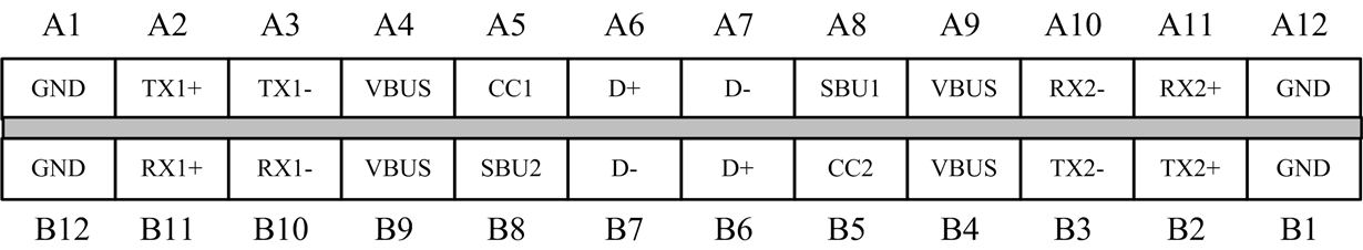
New roles and ports in USB Type-C

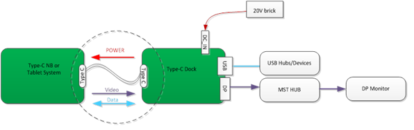
A new term making its debut along with USB Type-C is downstream-facing port (DFP). DFP refers to the port that we would commonly associate with the host. When you add the flexibility of power, the host is now able to negotiate data flow. In the default stage, the DFP sources VBus and the VCONN. Adding a Power Delivery (PD) controller allows for adaptation to fit the system’s needs. For example, users could have their phone act as a host, but still have power provided to it. A PD controller helps achieve this.

The converse is an upstream-facing port (UFP), which we would commonly associate with the device. In the default stage, the UFP sinks VBus and supports data. If the port is capable of doing either or both, then it is called a Dual-Role Port (DRP). A DRP can change dynamically. Enabling such versatile roles on a legacy connector (such as USB 2.0 or USB Standard A) requires complex controllers and software on the host and end device. However, the new 24-pin connector uses the configuration channel (CC) pin to comprehend which rows to identify between each adjoining side. TI’s TUSB320 family handles all of the USB Type-C channel controller and mode configuration for USB 2.0 and is available today.

USB Type-C is also future-proofed for higher data speeds, from the electrical capability of the connector and wiring to the standard that comprehends active cables. For active cables, there is a defined specification for VCONN – a 5V 200mA supply – that can power a signal conditioner in the cable for redriving or retiming.

The biggest area of advancement in the USB standard is Alternate Mode, which allows you to put a guest protocol on the cable. Alternate Mode allows for a guest protocol on the USB cable. This allows the users to exchange USB data, power and another protocol, which typically is video. There are several protocols from which to choose. The most widely known are DisplayPort (announced last September), Mobile High Link (MHL) (announced last November), Thunderbolt and PCI-Express. TI’s HD3SS460 USB Type-C cross-point switch supports Alternate Mode and is also available today.

New vocabulary just the beginning of the new standard’s impact

The adoption of USB Type-C will revolutionize how consumers interact with their devices, and it’s beginning to reshape our vocabulary surrounding its functions and implementation. Where do you expect to see USB Type-C and USB Power Delivery implemented over the next year? Log in to post a comment or question about the unique language of this new one-cable standard.

Additional resources


RF sampling: aliasing can be your friend

$
0
0

** This is the fourth post in a new RF-sampling blog series that’ll appear monthly on Analog Wire **

Communication system engineers are generally obsessed with signal-integrity issues. They want a low noise system to discern very small signals. They want high linearity performance to maintain immunity to interference. And when discussing high-sampling-rate data converters, their instinct is to sample at a very high speed in order to get many sample points within the period of the signal for best fidelity.

According to the sampling theorem, the minimum sampling rate must be at least twice the largest bandwidth of the signal. Sampling at speeds lower than the minimum results in aliasing. Ugh! This is bad, right? Not necessarily – aliasing can be your friend. Using an undersampling technique, you can use aliasing to your advantage and effectively mix a higher radio frequency (RF) down to a lower frequency captured by an analog-to-digital converter (ADC).

Take a look at the ordinary sinusoid shown in Figure 1a. The blue trace represents the ideal sinusoid signal. The red trace shows the discrete sample points of the ADC. In this example, there are five sample points per period of the signal. With those discrete points, there are actually an infinite number of frequencies that will intersect those exact same points. Figure 1b illustrates a frequency that is six times higher than the original signal yet still intersects the same sample points. The higher frequency will alias down to the ADC’s capture bandwidth. The ADC is acting like a conventional RF mixer in this case. With proper selection of the sampling rate, you can apply this undersampling technique to simplify the receiver architecture.

(a) Sinusoid signal with discrete sampling and (b) visualization of higher-frequency aliasing

Figure 1: (a) Sinusoid signal with discrete sampling and (b) visualization of higher-frequency aliasing

Another way to visualize the aliasing picture is to break the spectrum down into separate Nyquist zones. The first Nyquist zone represents the maximum sample bandwidth, which is equal to the sampling rate, Fs, divided by two. The higher Nyquist zones represent the adjacent spectrum bands with equivalent bandwidth. Figure 2 illustrates the Nyquist zone breakout. Visualize the spectrum folding back onto the first Nyquist zone like an accordion. Each signal that ultimately resides in the first Nyquist zone has a counterpart located in a higher Nyquist zone. With proper analog filtering, the ADC can capture a desired signal in one of the higher Nyquist zones, equivalent to a higher RF frequency.

Nyquist zones folding back

Figure 2: Nyquist zones folding back 

Although the sampling theorem states that any higher-frequency component can be aliased down, there is a practical constraint with the ADC’s sample-and-hold circuitry that limits its input bandwidth. The input-bandwidth constraint acts like a filter on the input. As signals exceed the input bandwidth, they will become attenuated to the point where the information is unusable; hence, input bandwidth is an important parameter to investigate when using undersampling.

As an example, the ADC083000 is an 8-bit, 3GSPS ADC with a 3dB input bandwidth of 3GHz. When operating at its maximum sample rate, this device supports signals up through the second Nyquist zone. The ADS5463 is a 12-bit, 500MSPS ADC with an input bandwidth of 2GHz. When operating at its maximum sample rate, this device supports signals up through the eighth Nyquist zone.

Check back for next month’s post, when I will discuss the advantages of cheating physics with oversampling.

Additional resources:


The secret to extending RS-485 communication performance

$
0
0

As many of you know, RS-485 is a physical layer standard used in all kinds of industrial and military standards. My colleague has a good series on RS-485 Basics on the Industrial Strength blog. In this post, I’ll touch on the basics from a little different angle and talk about how to get more range and speed from an RS-485 design.

RS-485 uses a differential pair of wires to allow a multiple-input, multiple-output (MIMO) configuration limited by upper-layer protocols residing in software. It is generally limited to 4,000 feet (about 1,200 meters) of cable and a maximum transmission speed of 10Kbps.

Assuming a single point-to-point model, the problem with going farther or faster (other than the driver/receiver limits) is the insertion loss of the cable. This is a function of length, cable inductance and dielectric loss. In general, the insertion loss appears as a low-pass filter and for many shielded twisted-pair cables used in harsh industrial environments will have roughly 2dB roll-off around 1MHz (per 100 meters) and 6dB roll-off at 10MHz (per 100 meters).

For a “bit” to be detectable without excessive jitter, edge transitions need to be fast and clean. If you perform a Fourier series on a square wave (a “101010 …” pattern of bits), you’ll see components that are appreciable well past the 11th harmonic. The insertion loss of 300 meters of cable will attenuate the higher frequencies, resulting in distortion.

If you try to use a standard RS-485 transceiver that can operate at 10Mbps (such as the SN75176B) to drive 300 meters of shielded twisted-pair cable, the high-frequency attenuation will slow the edge transitions, smearing the signal. At the receiver input, the signal will be greatly distorted from what was actually transmitted by the driver. Due to this distortion, there is uncertainty in when the receiver will detect an edge transition resulting in excessive jitter on the receiver’s output.

The typical ways to combat this problem are to equalize (or add an inverse loss function) before the receiver stage or pre-distort the driver output. Equalization circuitry adds gain at specific frequencies to flatten the cable’s transmission characteristics, resulting in an approximate flat response over the length of the cable. The loss function varies with cable type and distance, so you must adjust the amount of equalization – either by fixed values or dynamically through adaptive equalization. Pre-distortion (also called emphasis) either attenuates the lower frequencies (de-emphasis) or provides gain at the higher frequencies (pre-emphasis). This has a similar effect as equalization to flatten the cable response at the receiver.

Equalization and/or pre-distortion circuitry are prevalent in very high-speed (gigabit) transceivers, but rarely found in slower communication standards such as RS-485. However, TI has several extended-performance RS-485 transceivers such as the SN65HVD2x family (including the SN65HVD24). This family has several devices with built-in equalization on the receiver side of the transceiver.

Figure 1 shows a 5Mbps non-return to zero (NRZ) pseudo-random data pattern over 500 meters of twisted-pair wire. Trace 1 is the output of the driver stage, trace 2 is the signal at the input to the receiver after 500 meters of cable and trace 3 is the receiver output.

Figure 1: SN65HVD24 receiver performance at 5Mbps over 500 meters of twisted-pair cable

RS-485 transmission over larger distances and higher data rates is possible when using components that include circuitry to compensate for the cable losses. A great application note that goes into greater detail is “Use Receiver Equalization to Extend RS-485 Data Communications” by Clark Kinnaird. And if you’re trying to go faster and farther over RS-485, you might take a look at the SN65HVD2x transceiver devices.

Additional resources

How Ethernet technology is shifting modern markets 40 years after its inception

$
0
0

In my last blog post, “Three things you should know about Ethernet PHYs,” I discussed the evolution of Ethernet and the most essential information about the Ethernet physical layer transceiver (PHY). In this post, I’ll pick up where I left off and discuss how Ethernet PHYs are shifting modern markets.

Ethernet was invented over 40 years ago. Fast-forward through the standardization of IEEE 802.3 (10Mbps Ethernet PHYs) and into the world of 1995 – the era of “fast Ethernet,” where nominal data rates could reach up to 100Mbps. As part of this technological boom, National Semiconductor invented the industry’s first 10/100Mbps Ethernet PHY, a speed that’s still used predominantly even in today’s modern markets. What was even more impressive was the fact that National included a feature called auto-negotiation, which allowed the Ethernet PHY to operate at 10Mbps or 100Mbps without the need for human intervention. Both of these facets were considered a massive reinvention for Ethernet technology. As a result, new markets began emerging for the Ethernet PHY.

Figure 1: Ethernet PHYs are integrated into applications such as automotive diagnostics, robotic assembly lines and set-top boxes

In today’s markets, Ethernet technology is drastically changing the dynamics of how we efficiently transfer data. Ethernet PHYs are integrated into everything from automotive diagnostics to robotic assembly lines to set-top boxes, as shown in Figure 1. Ethernet PHYs are evolving to meet market demand due to three main factors:

  • Real-time communication
  • Robustness and reliability against external factors
  • Economical solution

Real-time communication

Today’s technological applications require electronics to provide a more real-time response. An Ethernet PHY architected and designed for such applications can provide improved link times and low latency. You can find an example of why low deterministic latency is important in a robotics assembly line. Robots need to be timed extremely precisely in order to optimize assembly time and reduce defects. If the Ethernet PHY did not have low deterministic latency, the processor would have to increase the delay between each action the robot takes. Multiplied hundreds or thousands of times, such delays would drastically increase assembly time and reduce throughput.

Robustness and reliability against external factors

Industrial and automotive equipment manufacturers have adopted the IEEE 802.3 Ethernet standard because of its functionality. To better address these markets, some suppliers have developed Ethernet PHYs that exceed the IEEE specification with extended temperature ranges, rigorous electrostatic discharge (ESD) testing, the ability to exceed electromagnetic interference (EMI) and electromagnetic compatibility (EMC) specifications, and excellent signal integrity. Ethernet PHYs are also undergoing stringent performance tests to become automotive qualified (AEC-Q100). Applications such as industrial data concentrators, industrial protective relays, and automotive gateways for on-board diagnostics and firmware upgrades all require robust testing.

Economical solution

Since Ethernet is a widely adopted and known standard, it is a cost-effective way to reliably transfer data quickly through a dedicated medium. This, along with Ethernet’s ease of use, has led to commercial products offering Ethernet connections such as set-top boxes, network printers and smart TVs.

In the meantime, where do you see Ethernet technology going in the next 10 years? Share your vision in the comments below.

Additional resources

USB Type-C does it all: Data, video and power delivery over a single cable connection

$
0
0

The recently released universal serial bus (USB) Type-C connector comes with many enhanced features. The connector is well-known to be “flippable” and reversible, and able to carry data, video and power over one connection. The specification defines the Type-C port so that it always supports USB, while you can enable Alternate Modes of operation such as DisplayPort video within the specification boundary defined for Alternate Modes. The USB Power Delivery (PD) protocol achieves enhanced power delivery up to 20V at 5A.

When the Type-C connector operates in USB-only mode without video or high power delivery, you will need a configuration channel (CC) controller and/or multiplexer (mux) switches. If you plan to enable extended features such as video and power delivery, you’ll need additional components such as a PD controller and a mux switch for signal mapping. You can enable the Type-C port with DisplayPort video and PD capability using TI’s PD and Type-C solutions: TPS65982 and HD3SS460.

The TPS65982 is a PD controller that is capable of handling CC logic for the Type-C connection protocol. It is also capable of managing the PD message handshake to enable extended features such as power delivery and video transfer. The TPS65982 comes with integrated power FET switches to handle power delivery over USB Type-C. It can also manage the external power FET to support power delivery up to 20V at 5A.

The HD3SS460 is a cross-point switch, enabling USB and PD signal paths based on the orientation and mode of the Type-C connection (which is determined by the PD contract between two connected systems). The PD contract determines the power and data roles. Note that if special features are enabled, the Type-C connector will not lose USB functionality.

You will need to identify Alternate-Mode devices over USB when PD messaging is not available. A new device class, USB Billboard, enables Alternate-Mode device identification over USB. The USB host should be able to access the USB Billboard and indicate the current mode of operation if the desired alternate mode can’t be enabled or updated. USB Billboard must be implemented on any USB Type-C devices with Alternate-Mode implementations.  The TPS65982 has an integrated USB2 end point to support USB Billboard.

The TI Type-C power and Alternate-Mode solution (TPS65982 + HD3SS460) supports all of the features I’ve described to enable enhanced VBUS power delivery and DisplayPort Alternate Mode.

Figure 1: Power contract and Alternate Mode negation between two ports

USB Type-C system implementation examples using TI’s Alternate-Mode USB Type-C solution include:

  • A notebook/tablet with a USB Type-C port supporting USB dual-role data, dual-role power and DisplayPort video output.
  • A docking station with a USB Type-C port supporting USB upstream-facing port (UFP), power source and DisplayPort sink.
  • A DisplayPort + USB dongle-type port extender with a Type-C port supporting USB UFP, power sink and DisplayPort sink.
  • A DisplayPort monitor with a USB Type-C port supporting USB UFP, power source and DisplayPort sink (monitor display).

Stay tuned to our USB blog series, including Roland Sperlich’s blog about “Why USB Type-C will make life easier,” for more information. Please leave us a note in the comments section below and let us know what other topics you would like us to cover.

Additional resources

Time-of-flight measurements using high-performance time-to-digital converters

$
0
0

On your mark, get set, go! Stopwatches are primarily known for their use at track or swim meets. Their accuracy generally does not extend beyond a millisecond, and you only need such specificity when the winner isn’t clear to the naked eye (also called a photo finish).

Several other applications need highly accurate stopwatches, however. In microelectronics, high-accuracy time-to-digital converters (TDCs) serve as stopwatches to take time-of-flight measurements; most engineers associate them with all-digital phase-locked loops (PLLs), where a TDC serves as phase detector. Various fields such as particle and high-energy physics have used TDCs for more than 20 years to take precise time-interval measurements.

There are several other use cases for TDCs. For example, radar systems require accurate stopwatches to track the speed of cars. Other examples can be found in the ultrasonic sensing space. In conjunction with ultrasonic sensors, stopwatches measure the time-of-flight (ToF) of an ultrasonic pressure wave passed through a medium. The time it takes for that pressure wave to return can measure distance, identify a medium, or detect contamination of a liquid. In other ultrasonic use cases such as flow meters, a stopwatch measures the delta time-of-flight (ΔToF, the difference between the time of flight upstream versus the time of flight downstream). Since you can derive critical information from a pressure wave’s ΔToF, the accuracy requirement of the stopwatch increases tremendously. In general, flow meters require stopwatch precision in the tens of picoseconds.

Magnetostrictive linear position sensors and light detection and ranging (LIDAR) sensors also use TDCs. In magnetostrictive applications, two superimposed magnetic fields interact with each other to give the position of the level sensor, which in this case is a magnet integrated into a float. The float is mounted upon a rigid wire made of magnetostrictive material. The transmitter electronics in the magnetostrictive level/position sensor generate pulses of current, thereby magnetizing the wire axially. The magnet on the float generates a torsional wave when it interacts with the field generated by the wire. One wave runs directly to the probe head, while the other is reflected at the bottom of the probe tube. The time-of-flight between the current pulse and the arrival of the wave at the probe head helps determine the position of the float. TDCs then convert this time-of-flight to digital signals to accurately measure the fluid level.

In LIDAR applications, you can measure the distance between objects by measuring the transit times between the generation of transmitted optical pulses and the receipt of the reflected waves. The actual calculation for measuring how far a returning light photon has travelsed to and from an object is quite simple (Equation 1):

 Distance = (Speed of Light x Time of Flight) / 2                      (1)

 Since the speed of light is a constant in a medium, by measuring the time of flight you can easily measure the distance.

But what else can you measure with an accurate stopwatch? Could you use a stopwatch to measure a voltage or current accurately? If you have not guessed already, the answer is yes. There is a popular analog-to-digital converter method called a slope integrator that entails the application of a voltage to an RC filter (a low-pass filter comprising a series resistor and a shunt capacitor to ground). A stopwatch measures the time it takes to charge the capacitor to a predetermined voltage level; you can compare that time to the time it takes for a known voltage reference to charge the same capacitor to the same voltage level. In this example, an accurate stopwatch and an accurate voltage reference yield high analog-to-digital conversion results.

With 50ps resolution and self-calibration, TI’s TDC7200 stopwatch supports ultrasonic sensing, magnetostrictive distance measurements, LIDAR, and analog-to-digital conversion of voltages and currents. In addition to its high accuracy, it is also very low power, which can benefit battery-operated applications such as ultrasonic flow meters.

TDC7200 has two measurement modes. Mode 1 can be used to measure ToF between 12ns to 500ns. In mode 1, TDC7200 performs this operation by counting from the START to the last STOP using its internal ring oscillator plus coarse counter. Figure 1 explains the measurement of TDC7200 in measurement mode 1.


Figure 1. Measurement mode 1 in TDC7200

In measurement mode 2, the internal ring oscillator of TDC7200 is used to count the fractional parts of the total ToF. The internal ring oscillator starts counting from when it receives the START signal until the first rising edge of the CLOCK. Then, the internal ring oscillator switches off, and the Clock counter starts counting the clock cycles of the external CLOCK input until a STOP pulse is received. The internal ring oscillator again starts counting from the STOP signal until the next rising edge of the CLOCK. This is shown in Figure 2.

Figure 2. Measurement mode 2 in TDC7200

Does your application require you to measure distances or fluid level/concentration? If so, you will need TDC7200 to perform the ToF measurements. Let us know by leaving a note in the comments section below.


Additional resources

Active RS-232 power consumption: Why isn’t it in the data sheet?

$
0
0

System designers will often not find active power consumption mentioned in a typical data sheet. Many RS-232 interface device data sheets only specify supply current for unloaded and shutdown setups. However, an RS-232 device is only useful for communications when connected to a remote RS-232 device. The data cable’s capacitance and remote receiver’s resistance are loads to the local RS-232 device that increase power consumption. While most new RS-232 devices will have at least one active current or power specification, there are many with none.

The active power consumption is the sum of the power consumed by the load and the power lost in the device. The first step is to calculate the load power for the receiver resistor and cable capacitance. Equation 1 is the remote receiver resistor power formula, expressed as the number of channels multiplied by driver voltage squared divided by receiver resistance.

N x V2 / R                                (1)

Equation 2 is the data cable’s power consumption expressed as driver peak-to-peak voltage squared multiplied by frequency and capacitance. The number of local RS-232 drivers doesn’t matter because only one driver toggles at a time.

F x C x (2 x V) 2                      (2)

The maximum frequency for a constantly toggling RS-232 data stream is half of the BAUD rate. The frequency for an arbitrary data stream is thirty percent of the BAUD rate.

The total load power is the sum of the resistive power (equation 1) and capacitive power (equation 2).

P = N x V2 / R + F x C x (2 x V) 2

For devices that don’t have capacitor- or inductive-charge pumps, the supply current needed for the load is the same as the load current. Supply and output current are directly proportional, just like a linear voltage regulator.

Therefore, you will need to convert the load power into a load current. Load current is load power divided by the driver voltage.

I = (N x V2 / R + F x C x (2 x V) 2) / V

This simplifies into equation 3, active load current.

I = N x V / R + 4 x F x C x V                   (3)

Use the active load current, which is same as supply current, to calculate supply power consumed as a result of the load. Add the no load power to get the total system device power

Here are two examples of how to calculate active supply power.

Example 1

The GD75232 transceiver has three drivers and five receivers. VDD = 9V, VSS = -9V and VCC = 5V. The maximum supply currents are 15mA, 15mA and 30mA. The maximum no-load power is 9V x 15mA + -9V x -15mA + 5V x 30mA = 420mW. This is a static (no load) power.

Data stream is 120k-baud alternating bit pattern, the cable capacitance is 2500pF and the remote receiver is 3 kilohms (kohms) resistance. RS-232 driver voltage is 7.5V.

Calculate the load current substituting example parameters into equation 3.

I = 3 channels x 7.5V/ 3000 kohms + 4 x 120kbps/2 x 2500pF x 7.5V = 12mA

Because this current comes from VDD or VSS, the supply power needed to support the load is 9V x 12mA = 108mW.

Total power is no-load (static) power – 420mW – plus the active power – 108mW – for a total power of 528mW.

Example 2

The TRS3232E multichannel RS-232 line driver/receiver has two drivers and two receivers. VCC = 5V. No-load ICC is 1mA maximum.

This device has a capacitor-charge pump that boosts and inverts voltage at the expense of current. If the data sheet had two specified loads, you could calculate the charge-pump efficiency, but it does not. In this case, you must measure active current empirically. Power consumption varies with frequency of the data stream and cable capacitance as well as receiver input resistance. See an example below:

Figure 1: TRS3232E power consumption vs. frequency, resistance 3 kohms/channel

Early TTL-based RS-232 devices did not have active-current specifications; that was OK because the active power was easy to calculate given the triple power-supply topology. Later single-supply charge pump RS-232 devices continued the “no specification for active power on the data sheet” mentality, but that’s a mistake, because you can’t calculate power from the data sheet alone. Visit the TI E2E™ community RS-232 forum for help wherever the data sheet doesn’t provide sufficient information.

Additional resources

Timing is Everything: Improving integer boundary spurs in fractional PLL synthesizers

$
0
0

Have you ever done a phase-locked loop (PLL) design with a fractional synthesizer that looked great at integer channels, but then the spurs got much higher on frequencies that were just slightly offset from those integer channels? If so, you have experienced the integer boundary spur, which occurs at an offset from the carrier equal to the distance to the closest integer channel.
 
For instance, if the phase-detector frequency is 100MHz and the output frequency is 2001MHz, the integer boundary spur would be 1MHz offset. In this case, 1MHz might be tolerable. But when the offset gets too small, but is still nonzero, the fractional spurs are worse.
 
Integer boundary spur reduction using a programmable input multiple
 
The concept of the programmable multiplier is to shift the phase detector frequency so that the voltage-controlled oscillator (VCO) frequency is far from an integer boundary. Consider a 20MHz input frequency used to generate an output frequency of 540.01MHz, as shown in Figure 1. The device has an output divider after the VCO, but both the output frequency and the VCO frequency are close to an integer multiple of 20MHz. This setup would stress any PLL for fractional spurs.


Figure 1: Integer boundary spur example

 If the device has a programmable input multiplier, then the configuration shown in Figure 2 is possible.

 
Figure 2: Avoiding integer boundaries using a programmable multiplier
 
Figure 3 shows the impact of the internal multiplier. Integer boundary spurs have multiple mechanisms, and it is difficult to completely eliminate them. But this method both reduces the integer boundary spur as well as other spurs that spawn from it.
 
The “spur-b-gone” trace in Figure 3 shows the impact of using this programmable multiplier. There’s an approximate 9dB reduction in the integer boundary spur at 100kHz, while substantially reducing other spurs at 50kHz and 10kHz.
 

Figure 3: Spur comparison with and without programmable multiplier
 
The examples shown were done with the TI’s LMX2571 synthesizer, which includes a programmable multipler that requires no external components. This device also features 39 mA current consumption, a PLL figure of merit of -231 dBc/Hz, and a continuous output frequency range of 10-1344 MHz. It can support applications including land mobile radios, software-defined radios and wireless microphones.

 Additional resources


IBIS-AMI channel simulations made simple through WEBENCH Interface Designer

$
0
0

High-speed serial-link simulations are powerful tools for signal-integrity engineers. These simulations give designers a glimpse of system performance prediction, allowing them to more easily make good decisions to meet design goals before committing a design to expensive board fabrication.

TI’s WEBENCH® Interface Designer offers a simple yet powerful environment for serial-link simulations. This free Web-based tool serves as a quick and easy-to-use first step in high-speed channel analysis – a supplement to the more rigorous and time-consuming analyses traditionally performed by licensed electronic design automation (EDA) software tools. You can read more about WEBENCH Interface Designer in this blog post.

This all sounds great, but will the tool give you reliable results? To answer this question, I went to the lab and made some measurements. I decided to use a 12.5 Gbps linear redriver DS125BR820EVM, some FR4 printed circuit board (PCB) traces and breakout boards with SMA connectors for a back-plane sub-system. Figure 1 illustrates my simple setup. A bit error rate tester (BERT) acts as the transmitter as well as the receiver for this study.


Figure 1: Lab measurement setup

First, I measured the S-parameters of all the cables, connectors and board trace using a four-port network analyzer and saved them to be used as channel models. I then cascaded these files to create combined models for a pre-channel (anything before the device) and a post-channel (anything after the device) for uploading into WEBENCH Interface Designer. The input/output buffer information specification-algorithmic modeling interface (IBIS-AMI) model of the DS125BR820 is accessible from the tool, so the last thing to do is set up the transmitter. I used a generic IBIS-AMI transmitter model and matched the edge rates and differential-output voltage as closely as possible to the BERT. Now that my WEBENCH environment replicates my lab bench, I can run simulations for several different settings and see how well they match. Another neat thing about WEBENCH Interface Designer is that it processes the simulations remotely, so I can run them on my notebook computer in the lab without having to worry about processing power.

Two cases were used in this study. Case 1 is the use of PCI Express Gen 3 at a data rate of 8Gbps. Case 2 is the use of SAS Gen3 at a data rate of 12Gbps.

The specifications for case 1 were:

  • BERT output: 8Gbps, 800mVpp.
  • Channels: ~10dB at 4GHz pre-channel, ~2dB at 4GHz post-channel.
  • DS125BR820 settings: Input equalizer level 3, output amplitude level 5.

 Figure 2: Lab data (left) and WEBENCH Interface Designer simulation data (right) for case 1

 The specifications for case 2 were:

  • BERT output: 12Gbps, 800mVpp.
  • Channels: ~14dB at 6GHz pre-channel, ~3dB at 6GHz post-channel.
  • DS125BR820 settings: Input equalizer level 4, output amplitude level 7.


Figure 3: Lab data (left) and WEBENCH Interface Designer simulation data (right) for case 2

The DS125BR820 opens the eye at the output of my system. Case 1, illustrated in Figure 2, shows me that I have plenty of margins and can likely tolerate more channel loss while still maintaining an open eye. Case 2, illustrated in Figure 3, shows the opposite; my channel has too much loss and I am likely going to see bit errors at these operating conditions unless additional equalization is applied at the end of the channel.

If you do not have S-parameter measurements to upload like I did, you can simply type in the expected loss at a given frequency; WEBENCH Interface Designer will generate generic S-parameters that match your desired insertion loss.

Setting up and running a simulation like this takes about 30 minutes and produce reasonable well-matched result compared with laboratory measurements. The WEBENCH Interface Designer is a very useful web-based tool to help users to pick the right device based on their applications requirement. I hope you’ll give it a try!

Let us know if you have any suggestions or comments on WEBENCH Interface Designer by logging in to post a comment below.

Additional resources

NVME and PCI Express: What’s the difference?

$
0
0

When you ask a bunch of hardware engineers, “What is NVME?,” you might get the following responses:

“NVME is an acronym for ‘nonvolatile memory express’.”

  • “NVME is the best thing to ever happen to solid-state storage!”
  • “I think NVME is, uh, related to PCI Express?”

While these answers are all essentially correct, they won’t help you build a storage system that leverages the advantages of this game-changing new technology. Texas Instruments has many years of experience in the hardware behind PCI Express (PCIe) and enterprise storage, and we can share insight into this important technology and how it impacts future hardware designs. Here’s how I would answer the question:

“NVME is a protocol developed explicitly for solid-state memory. While Serial Advanced Technology Attachment (SATA)remains the heavyweight champion of storage protocols, it wasn’t built to deal with solid-state storage and can’t offer the advantages of NVME.”

In order to explain SATA and NVME, let’s compare them to a physically similar counterpart: a record player. In order to play music, a turntable needle reads information from a record and outputs that data to speakers. SATA hard drives allow their “records” to spin up to 15,000rpm while reading data over a read/write head; like a record player, the architecture relies on a single needle. In comparison, NVME running on a solid-state drive (SSD) is more like an MP3 file. All of the data is laid out in a readable format, and can be read by as many as 64,000 parallel “needles” at the same time.

When it comes to transporting your data, SATA is also a physical bus, like the wire between your music player and speakers. Traditionally, it hasn’t been the bottleneck for storage drives, but a faster bus like PCIe could “boost” the maximum achievable speed.

Why should I care about NVME?

In terms of input/output (I/O) operations per second (IOPS), typical hard-disk drives range in the low hundreds, while NVME SSDs post numbers in the hundreds of thousands to millions of IOPS. In terms of read and write speeds, SATA hard disks support several hundred megabytes per second, while NVME supports several gigabytes per second – one order of magnitude greater. All of this translates to unparalleled performance gains.

How do I build NVME?

OK, so you get it – NVME is fast. But this is a guide for hardware engineers, right? So far, we’ve been describing the car without talking about the road it’s driving on. Fortunately for everyone, the answer is very simple: the PCIe bus.

NVME is a storage protocol, but the physical layer that NVME runs on is plain old PCIe. This means that hardware engineers can leverage existing resources to check compliance, use existing reference designs, and simulate with existing modeling tools. It also means that products qualified by the PCI Special Interest Group (SIG) to support PCIe Gen 3, like DS80PCI810, can support NMVE applications.

Fig 1: DS80PCI810 PCIe Gen 3 redriver typical application block diagram

As I mentioned earlier, TI has turned decades of industry experience into reference designs and resources to get your system off the ground today. TI can also deliver all of the components to develop next-generation PCIe NVME drives, from power to signal chain.

Now that you know the basics of NVME and PCIe, leave us a note below and let us know what other topics related to PCIe you would be interested in hearing about.

 Additional resources

Improve Class-D EMI to downsize BOM cost without compromising audio performance

$
0
0

Designers frequently choose Class-D audio amplifiers to drive the speakers in a variety of mid-power applications like TVs, Bluetooth® speakers and laptops. After all, when compared to conventional Class-AB, Class-D has lower heat dissipation and relatively high efficiency (for increased battery life). Class-D is also beneficial if compact board space is important.

The biggest challenge associated with Class-D is electromagnetic interference (EMI). External inductor-capacitor filtering is traditionally used to mitigate EMI, but it adds cost, area and complexity to end equipment.

TI has developed several closed-loop amplifiers including the TPA3110 (released in 2010), which made significant improvements to EMI by using advanced closed-loop power stages. TI has also just released the TPA3140 Class-D audio power amplifier, which includes several innovations that help provide true inductor-free performance even for speaker cables up to 1m in length. This inductor-free device is already in production in LCD TVs, where long speaker cables make meeting EMI requirements a challenge.

Edge-rate control

One method used to reduce EMI radiation is to reduce the slew rate of the amplifier output transitions. Since the TPA3140 uses a proprietary high-performance feedback topology, a reduction in slew rate will not degrade total harmonic distortion (THD) or audio quality. The fast Fourier transform (FFT) image in Figure 1 shows a reduction in high-frequency content with slower edges.

EMI plots without edge rate (red) and with edge rate (yellow)

Figure 1: EMI plots without edge rate (red) and with edge rate (yellow)

Spread-spectrum clocking

While edge-rate control is an effective means of attenuating EMI when it arises in frequency ranges greater than 30MHz, it does not address the fundamental carrier frequency of the Class-D amplifier’s switching output and its related harmonics, which fall in the range below 30MHz.

The TPA3140 includes a proprietary algorithm that adds a small amount of frequency modulation to the amplifier’s clock circuitry. This algorithm doesn’t affect the amplified audio quality, but significantly reduces peak energy of the switching frequency.

EMI results

Figure 2 represents EMI test results from a TV with a close to 1m speaker cable length. The red line is the quasi-peak limit, and the green line is the average limit.

EMI plot:  blue quasi-peak and green is average curve

Figure 2: EMI plot:  blue quasi-peak and green is average curve

Audio performance:

  • <0.05% THD+N at 1 W/4 Ω/1 kHz
  • <65-µV A-wgt output noise

In conclusion, the TPA3140 Class-D audio power amplifier provides significant improvement in EMI that allows inductor-free operation providing major BOM cost savings without compromising audio quality.

Additional resources

Get Connected: Failsafe bias those contentious buses!

$
0
0

Welcome back to the Get Connected blog series on Analog Wire. In my previous post, I discussed how to use low-voltage differential signal (LVDS) transceivers as a high-speed comparator in a few different applications. In this post, I’ll cover failsafe biasing of differential buses and how to implement failsafe biasing in your next design.


Bus topologies that implement more than one driver and receiver on the bus – known as multipoint – present challenges to system designers given their difference from a point-to-point bus topology. (To review bus topology architectures, see my previous blog post, “LVDS for multipoint applications.”) In multipoint applications, bus contention and idle bus conditions can cause collisions or communication glitches on the bus during normal operation. Bus contention occurs when more than one driver is active while the bus is in an indeterminate state; idle bus conditions occur when all of the drivers are in the off or Hi-Z state. The implementation of a failsafe biasing network addresses both of these situations.

A bus that implements failsafe biasing only has two logic states in which it can exist – high and low –while a bus without failsafe biasing can exist in unknown states. An active driver will drive the bus high and low or bias it to a known state through the failsafe biasing network. Without a failsafe biasing network, the bus will reside in an unknown state in which the receiver output is invalid; noise can couple through the transceiver, causing false transitions. Figure 1 shows the possible states of a typical RS-485 bus with and without failsafe biasing.

Figure 1: RS-485 bus states

Failsafe bias resistor values are based on the maximum receiver threshold levels of the transceiver devices used in the end application, like the SN65LBC180 RS-485 transceiver. Typically for a RS-485 network the receiver input threshold level is ±200mV and for an LVDS network it is ±50mV. In addition to the receiver threshold levels, the termination resistors RFS1 and RFS2 should be equal, as that provides symmetrical loading for the drivers. The equivalent resistance of RFS1, ZT1 and RFS2 should match the characteristic impedance of the twisted-pair cable or printed circuit board (PCB) trace to maintain signal integrity (ZT1||(RFS1 + RFS2). ZT2 should also match the characteristic impedance of the network, also to maintain signal integrity, by reducing reflections on the network. Figure 2 shows a multipoint bus topology with failsafe biasing implemented.


Figure 2: Differential bus with failsafe biasing

For more information on failsafe biasing, please see the application note, “Failsafe Biasing of Differential Buses.” Leave a comment below if you’d like to hear more about anything discussed in this post, or if there’s an interface topic you’d like to see in the future.

 Additional resources

Inductive sensing: How to design an inductive sensor with the new WEBENCH Coil Designer

$
0
0

Designing coils for inductive sensing may initially appear like a daunting task, but the WEBENCH® Coil Designer makes the process very simple.

If you have designed with TI's inductance-to-digital converters (LDCs), then you may have already used WEBENCH Designer for Inductive Sensing Applications, which suggests suitable coils for given input parameters and exports them to PCB CAD tools.

Figure 1 is a screenshot of our second inductive sensing WEBENCH tool. WEBENCH Coil Designer designs custom sensor coils for applications where you already know the system constraints. It supports real-world PCB manufacturing constraints such as adjustment of trace geometries and PCB thickness.

Both toolsexport the resulting coil directly to popular PCB layout tools and allow complete sensor coil design in only five minutes.

Figure 1: WEBENCH offers two tools for inductive sensing

You can design a custom sensor coil in five simple steps:

1.Select LDC Device: Let’s use the LDC1612 to design a coil. While this selection does not impact the coil directly, we recommend selecting the most appropriate LDC because WEBENCH Coil Designer considers device-specific boundary conditions during its calculations (Figure 2).

Figure 2: WEBENCH Coil Designer displays and considers device-specific boundary conditions

2.Select Coil Type: WEBENCH Coil Designer supports four coil types. Circular coils are used for most applications because they offer a higher Q-factor than the other choices, but sometimes system geometry requirements and sensor inductance requirements dictate the use of square coils. Figure 3 defines inner and outer coil diameter, trace width and trace spacing.

Figure 3: WEBENCH Coil Designer supports circular, hexagonal, octagonal and square coil

3. Select Coil Geometry and Other Parameters: In this window, I specified the physical coil properties such as the number of turns, PCB layers and trace geometries, as shown in Figure 4.

Trace width and trace spacing affect the manufacturing cost; narrower traces and spacing typically result in more expensive PCBs. The outer coil diameter has the largest impact on the maximum sensing range. A coil fill ratio (inner diameter / outer diameter) of ≥ 0.3 is recommended. Typically, smaller coil fill ratios do not improve performance because the innermost turns add little inductance compared to the increase in AC resistance, and therefore have a reduced Q-factor. The “view more” option shows advanced information about the sensor.


Figure 4: Output parameters for given coil geometries. Clicking ‘View more’ displays advanced output parameters

The WEBENCH tool displays a warning if violations of device-specific boundary conditions or recommendations occur. For example, a sensor with an oscillation frequency of 8MHz is suitable for the LDC1612, but not for the LDC1000, which has a maximum sensor frequency of 5MHz (Figure 5).

Figure 5: Designing an 8MHz sensor for the LDC1000 produces a warning and recommendation for avoiding the system constraint

4. Output Graph: The window in Figure 6 shows the sensor characteristics based on the inputs in step 3. The tool generates a wide range of plots after you select the desired parameters from the drop-down menus, and compares the performance of different coil types.

Figure 6: Output parameters plotted against input parameters and compared to different coil types

5. Export Design: Finally, you can export the coil design into one of five different PCB CAD tools, as shown in Figure 7.

Figure 7: The export function exports the coil into PCB layout software

I exported the coil to the Altium Designer format and open the resulting file, as shown in Figure 8.

Figure 8: The resulting sensor coil when imported into Altium Designer

The new WEBENCH Coil Designer complements the WEBENCH Inductive Sensing Designer by offering more control over the physical coil properties.

Do you find our WEBENCH tools for inductive sensing useful? Are there other WEBENCH tool features that would make your system design with LDCs easier? If so, leave a note in the comments section below.

Additional resources

RF Sampling: How over-sampling is cheating physics

$
0
0

** This is the fifth post in a new RF-sampling blog series that’ll appear monthly on Analog Wire **

RF sampling converters can capture high-frequency signals and large-bandwidth signals; however, not every application utilizes signals that require very high-speed sampling. For cases where the bandwidth or the output frequency is not excessive, there is still an advantage to utilizing the high sampling rate capabilities of RF sampling converters.

The sampling theorem states that the sampling rate must be at least twice the largest bandwidth of the signal. Sampling below this rate is called under-sampling and causes aliasing; the benefits of this approach were discussed in my previous blog. Sampling above this rate is called over-sampling. Over-sampling offers some processing advantages that seemingly let you defy physics.

One of the key measurement parameters for analog-to-digital converters (ADCs) is signal-to-noise ratio (SNR). SNR measures the relative level between the desired signal power and the entirety of the noise power within the first Nyquist zone. The Nyquist zone bandwidth is the sampling rate divided by two (Fs/2). Recall that all signals and noise will fold back into the first Nyquist zone. This zone effectively represents the entire bandwidth of the device.

One benefit of over-sampling is that the image components are separated farther in frequency space. This allows easier analog filtering to eliminate interfering signals that can alias down into the captured bandwidth and desensitize the receiver. Figure 1 illustrates two cases: one signal sampled near the Nyquist rate and one that is over-sampled. The over-sampled case provides a more realizable analog anti-aliasing filter.

Figure 1: Filter impact for Nyquist rate sampling vs. over-sampling

Over-sampling can improve the SNR performance of the device beyond the theoretical quantization noise limitations. The quantization noise is equally distributed across the Nyquist bandwidth. By increasing the sampling rate, the same quantization noise is spread over a larger Nyquist bandwidth. The desired signal remains fixed. Decimation coupled with digital filtering decrease the noise bandwidth without impacting the desired signal. Note, decimation implies over-sampling since there must be additional samples available to remove. In RF sampling ADCs, it is more common to refer to a decimation factor rather than an over-sampling rate; however, these parameters are effectively equivalent.

For example, decimating by two must have the signal over-sampled by at least two. In this example, the signal power remains the same but the Nyquist bandwidth is cut in half. This eliminates half of the noise power, which improves the ADC SNR by 3 dB. The first equation represents the ideal SNR due to quantization noise where N is the number of bits of the converter. The second equation represents the SNR improvement related to the decimation factor D.

From a pure quantization noise analysis, each fourfold increase in sampling rate equates to one effective bit of resolution improvement. In theory, a 12-bit data converter can achieve the SNR performance of a 16-bit converter by sampling at 16 times the minimum Nyquist rate. In practice, RF sampling data converters do not achieve SNR performance equivalent to the quantization noise limit due to other impairments related to aperture jitter, clock jitter and thermal noise; however, the over-sampling technique still provides nearly the same relative SNR improvement. In many communication systems, this benefit is critical. For example, the ADS54J60 is a 16-bit, 1-GSPS ADC that has options for decimation by two or four. The designer can make the decision to increase the sampling speed and introduce decimation in order to improve the SNR performance.

Check back next month when I will discuss the details of the digital mixers in RF sampling data converters.

Additional resources

Offset correction improves the next generation of heart-rate smart watches

$
0
0

You don’t need to look too hard to find complaints about the accuracy of optical heart-rate smart watches. Many technology blog reviews stated that you’ll benefit from its activity and sleep-tracking functions rather than the optical heart-rate monitor to achieve your health and fitness goals.

When optical heart-rate technology was first introduced, accuracy issues seemed to put a damper on the significance of this technology in being able to improve health and fitness for many consumers. The reason the accuracy of the optical heart-rate readings were so far off was because our human anatomy puts forth several significant challenges.

For an optical heart-rate monitor to work, an accurate AC reading from the photodiode is necessary. However, it is very difficult to get a reading of the AC since there is so much DC output from outside the system. DC offset correction gives you the ability to read the AC waveform with minimal performance issues from the DC output. The way this technology works is that an offset subtraction digital-to-analog converter (DAC) eliminates any DC noise coming from sources like ambient light. There is also some correction needed from the DC noise coming from the skin and arteries. With this offset subtraction DAC, you can get a better reading of the AC waveform and amplify the remaining signal for high gain and more accuracy, as shown in Figure 1.


Figure 1: DC offset correction for higher gain

Another problem of early optical heart-rate watch models was that sweat or any kind of wetness on the skin caused inaccurate readings, severely limiting the watch’s efficiency. The solution was to place a piece of glass in-between the watch’s light-emitting diodes (LEDs) and the skin to isolate the wetness. However, the reflection from the glass between the skin and the LEDs led to crosstalk, again creating noise inaccuracies in the heart-rate readings, as shown in Figure 2.


Figure 2: Crosstalk between ambient light, glass and LEDs on the bottom of a smart watch

In a study case done in the TI lab, we tested a watch design with no glass barrier and no DC correction in place and measured an AC output of 3.5mV. When we added just the glass, the AC output went down to 2mV and was sometimes unattainable. Finally, we introduced TI’s AFE4404 analog front end (AFE) for wearable, optical heart-rate monitoring and bio-sensing. The AFE4404 offers a feature for DC offset correction that mitigates crosstalk through its ability to isolate important AC signals from the DC noise. In our last test, we measured an AC output of 15mV, close to five times better than first case and seven times better than the second case.

Offset-correction technology solves several accuracy issues in optical heart-rate designs and improves the performance of optical heart-rate smart watches. With this technology from TI, we expect users will be a lot happier with their optical heart-rate technology!                                             

Additional resources


What are you sensing? Pros and cons of four temperature sensor types

$
0
0

Choosing temperature-sensing products may seem trivial, but with the wide variety of products available, this task can be quite daunting. In this blog post, I’ll present four types of temperature sensors – resistance temperature detectors (RTDs), thermocouples, thermistors and integrated circuit (IC) sensors with digital and analog interfaces – and discusses the pros and cons of each.

From a system-level standpoint, the right temperature sensor for your application will depend on the required temperature range, accuracy, linearity, solution cost, features, power consumption, solution size, mounting (surface mount vs. through-hole vs. off-board) and ease of designing the necessary support circuitry.

RTDs

When measuring the resistance of an RTD while varying its temperature, the response is almost linear, behaving like a resistor. As shown in Figure 1, the RTD’s resistance curve is several degrees out of linearity (with a straight line shown for reference) but is highly predictable and repeatable. To compensate for this slight nonlinearity, most designers digitize the measured resistance value and use a lookup table within the microcontroller to apply correction factors. This repeatability and stability over a wide temperature range (roughly -250°C to +750°C) makes RTDs useful in high-precision applications, including measuring temperature of fluid or gas in pipes and tanks.

Figure 1: RTD resistance versus temperature

The complexity of the circuitry to process the RTD analog signal varies substantially based on the application. Components such as amplifiers and analog-to-digital converters (ADCs), which generate their own inaccuracies, are necessary. You can also achieve low-power operation by powering the sensor only when a measurement is necessary, but this complicates the circuitry even more. Plus, the power required to energize the sensor also raises its internal temperature, which affects measurement accuracy. With only a few milliamps of current, this self-heating effect can develop temperature errors that are correctable but require further consideration. Also, keep in mind that the cost of a wire-wound platinum or thin-film RTD can be relatively high, especially when compared to an IC sensor.

Thermistors

A thermistor is another type of resistive sensor. There are a wide variety of thermistors available, from inexpensive to high-precision products. Low-cost, low-precision thermistors perform simple measurement or threshold-detection functions; require multiple components (such as a comparator, reference and discrete resistors); are very inexpensive; and have nonlinear resistance-temperature properties, as shown in Figure 2. If you need to measure a wide range of temperatures, you will need substantial linearization. Calibrating to several temperature points may be necessary. For better precision, more expensive and tighter tolerance thermistor arrays are available to help overcome this nonlinearity but are generally less sensitive than single thermistors.


Figure 2: Thermistor resistance versus temperature

Because of the increased complexity and cost of multiple trip-point systems, low-cost thermistors are typical only in applications with minimal functionality requirements, including toasters, coffee makers, refrigerators and hair dryers. Thermistors also suffer from self-heating, usually at higher temperatures where their resistances are lower. As with RTDs, there are no fundamental reasons why you cannot use thermistors with low supply voltages – keeping in mind that the full-scale output is lower, which translates directly to less system sensitivity based on the analog-to-digital converter (ADC) characteristics. Low-power applications also require increased circuit complexity to be sensitive to noise-induced errors. Thermistors operate in the -100°C to +500°C temperature range, although most are rated for maximum operating temperatures between +100°C and +150°C.

Thermocouples

A thermocouple consists of a junction of two wires made of different materials. A Type J thermocouple, for example, is made from iron and constantan. As shown in Figure 3, junction 1 is located at the temperature to be measured, while junctions 2 and 3 are kept at a different temperature measured with an LM35 analog temperature sensor. The output voltage is approximately proportional to the difference in these two temperature values.

Figure 3: Using the LM35 for thermocouple cold-junction compensation

Because a thermocouple’s sensitivity is rather small (on the order of tens of microvolts per degrees Celsius), you would need a low-offset amplifier to produce a usable output voltage. Nonlinearities in the temperature-to-voltage transfer function over a thermocouple’s operating range often necessitate compensation circuits or lookup tables, as with RTDs and thermocouples. However, despite these drawbacks, thermocouples are very popular, particularly for ovens, water heaters, kilns, test equipment, and other industrial processes, because of their low thermal mass and wide operating temperature range, extending beyond 2300°C.

IC sensors

IC sensors can operate within a temperature range from -55°C to +150°C – a select few can go as high as +200°C. There are various types of integrated IC sensors, but the four most common are analog output devices, digital interface devices, remote temperature sensors, and those with thermostat functionality (temperature switches). Analog output devices (usually a voltage, but some with current outputs) are most like passive solutions in their need for an ADC to digitize the output signal. Digital interface devices most commonly use a two-wire interface (I2C or PMBus) and have an ADC built in.

Aside from also including a local temperature sensor, remote temperature sensors have one or more inputs to monitor a remote diode temperature, which are most often located in a highly integrated digital IC (for example, a processor or field-programmable gate array [FPGA]). Thermostats provide a simple alert when a temperature threshold is reached.

There are many benefits to using IC sensors, including low power consumption, package offerings (some as small as 0.8 mm x 0.8 mm) and low device cost in certain applications. Furthermore, since IC sensors are calibrated during production testing, there is no need to calibrate further. They are often used in fitness tracking, wearables, computing systems, data loggers and automotive applications.

Savvy board designers will make use of the most appropriate solution depending on the end product requirements. Table 1 shows the relative advantages/disadvantages of each type of temperature sensor.


Table 1: The relative advantages and disadvantages of RTDs, thermistors, thermocouples and IC sensors

Stay tuned for more temperature basics blog posts from me and my colleagues in the coming months. Please comment below and let us know if there are any topics you would like us to cover.

More resources

How to easily move from USB 2.0 to USB Type-C

$
0
0

Are you excited about moving your USB 2.0 (or USB 1.1) application – such as a flash drive, charger, power adapter, external drive or hard drive – to the USB Type-C reversible connector? Here’s a guide to easily migrate your USB 2.0 Type-A, Type-B or micro-A peripheral, host or On-The-Go (OTG) design to Type-C.

The connector

Figure 1 shows the receptacle pin assignment for supporting a full-featured Type-C cable that supports both USB 2.0 and USB 3.1.

Figure 1: USB Type-C full-featured receptacle pin map (front view)

 When migrating from a USB 2.0 product to a Type-C product, you will not need the USB 3.1 signals, so leave them unconnected (electrically isolated) on the printed circuit board (PCB). Figure 2 shows the USB 3.1 contacts as no-connects (NC) in a Type-C receptacle.

Figure 2: Receptacle pin map with USB Type-C USB 2.0 (front view)

 The pin map in Figure 2 has two sets of D+ and D- contacts. These two sets of pins do not imply that there are two independent USB 2.0 paths. In fact, a USB Type-C cable has only one wire for D+ and one wire for D-. The purpose of these two sets of D+/D- contacts is to support the “flippable” feature. Products should connect both the two D+ contacts together as well as the two D- contacts together on their PCB. When tying these contacts together on the PCB, creating a stub is unavoidable. As such, be careful that the stub length does not exceed 2.5mm. Otherwise, you may notice signal-integrity issues on the USB 2.0 interface.

Noticeably absent from the USB Type-C receptacle is the ID pin of the older Type-A and Type-B connectors. The determination of host or peripheral functionality is handled differently in Type-C using the configuration channel (CC) pins. The CC pins perform the same functions that the ID pin previously performed; they indicate the role of equipment as host, peripheral or both. The CC pins also detect if the connection is being made or if it is broken; and a few additional things not required when implementing USB 2.0 on Type-C.

One-chip solution

You can transition a USB 2.0 host, peripheral or OTG product that uses a micro-A/B receptacle to a USB Type-C receptacle with one device – the TUSB320. This family of devices can function as an upstream-facing port (UFP), downstream-facing port (DFP) or a dual-role port (DRP) product based on a pin or value of an I2C register. The device handles all aspects of the USB Type-C connection process, (including the CC pins that mirror the micro-A/B ID pin behavior) for easy determination of the DFP or UFP role.

When connected as a peripheral (UFP), the TUSB320 indicates the VBUS current provided by the attached host through either I2C registers or general-purpose input/output (GPIO) pins. When connected as a DFP, these devices advertise VBUS current to the attached peripheral.

Are you moving to USB Type-C? If so, what application are you migrating? Let us know in the comments section below.

Additional resources

Read TI’s white paper


Tips and tricks for human body temperature measurement with analog temperature sensor ICs

$
0
0

Technological advancements have allowed temperature sensor integrated circuits (ICs) to be used for precision applications such as human body temperature measurement found in wearable health bands and medical devices. TI’s temperature sensing team has received many questions regarding these types of applications with the recent release of the accurate, small-form-factor LMT70 analog temperature sensor for human body temperature measurement. As I have answered some of these questions in the past with other sensors, I thought I would cover a few in this post.

Q: When monitoring a sensor with an analog-to-digital converter (ADC), how can you achieve better quantization error with a 12-bit ADC, such as the one found in MSP430™ ultra-low-power microcontrollers (MCUs)?

A: Using rolling averages in the software can improve the resolution of the ADC – you can actually change the number of averages and see that the noise level as well as the resolution increase or decrease. Rolling averaging works if the noise amplitude of the signal applied to the ADC input is greater than the ADC’s least significant bit (LSB). For example, using a rolling average of 16 samples extends 12-bit ADC resolution to 14 bits using Equation 1:

                      (1)

The LMT70 evaluation module uses the MSP430 MCU’s 12-bit ADC. The typical performance of this evaluation module has shown to be ±0.07°C due to this technique.

Q: How does the transfer function affect the overall accuracy of the analog temperature sensor?

A: There are accuracy curves in many datasheets that show how different equations affect accuracy. Regarding the LMT70, with second- or third-order curves, the accuracy is about the same as the lookup table (LUT) for the limited temperature range of human body temperature measurement, so the device will meet the same specifications. Of course, as the curves show in Figures 1 and 2, the third-order equation given in the data sheet for 10°C to 110°C is best to use. Even a second-order curve that is best fit for 20°C to 45°C may give acceptable results.

How do you generate this equation? Use Excel or MATLAB curve fitting. And how do you generate the accuracy curves? Simply plug in the minimum and maximum voltage limits found in the data sheet’s electrical characteristic (EC) table into your equation.

Figure 1: Using a third-order transfer-function best fit, 10oC to +110oC

Figure 2: Using a second-order transfer function best fit, 10oC to +110oC

Q: Can a battery that varies from 1.8V to 3V directly power an analog sensor, and what is the impact on accuracy?

A: Analog sensor datasheet specifications include power-supply sensitivity as well as curves so that you can determine the impact on accuracy. Let’s look at the LMT70 as an example. Figure 3 (from page 9 of the LMT70 datasheet) shows a typical curve found in analog temperature sensor datasheets.

Figure 3: LMT70 line regulation

As you can see, accuracy down to 2V is very good for a typical LMT70 sensor. Each division in this curve is 0.5mV, so that is 0.1°C. The power-supply sensitivity limit is +/-9m°C/V. Thus for a range of 2V to 3V, you get a variation of no more than 0.009°C. For a target of 0.1°C-0.2°C, the impact on error is negligible.

All ICs have a voltage level where they start to malfunction or turn off. For the LMT70, this occurs below 2V, as listed on the EC table. If you try a few LMT70 sensors on the bench, you may find that some work below 2V, but TI does not specify the IC for that voltage. IC manufacturers do extensive characterization on devices to ensure that datasheet specifications cover future production variations.

Q: Electrostatic discharge ESD – Do I need to be worried about it?

A: If you are worried about the ESD at connectors and those connectors will be user-accessible, you need to protect both the MCU board and the IC sensor, as shown in Figure 4 in red. You could also add notes in the user’s guide warning about using ESD safe practices when handling the boards/assemblies.

  Figure 4: Sensor placed off board

If users won’t be able to access the connector, the analog temperature sensor should be handled in an ESD-safe environment. For the LMT70 specifically, no additional ESD protection is necessary, as this sensor has built-in ESD protection for manufacturing purposes.

Please leave us a note below and let us know what else you would like to know about IC temperature sensors—perhaps we’ll answer them in a future blog post!

Additional resources

It’s all in the family: a brief guide to logic family selection

$
0
0

Virtually every electronic system needs a logic device of some kind. And with TI’s large portfolio, we’re able to help with just about any logic need. But with all those devices to choose from, it can sometimes be daunting to choose the correct logic device for a design. Knowing the exact logic function and voltage range you’re looking for helps, but there still may be many devices that generally fit your criteria. So let’s discuss why TI has so many different options, and how to choose the right one for your design.

I’m going to assume that you are familiar with logic terminology such as propagation delay and output drive strength. If you need to brush up a bit, please check out our application note, “Introduction to Logic.”

So, what’s a logic family? A logic family is a group of unique logic devices that operate on a particular technology. For example, the HC family comprises many parts, including negative-AND (NAND) (SN74HC00) gates. You can find NAND gates in practically every logic family we make. For a couple of examples, take a look at the LV family (SN74LV00A) and the AUC family (SN74AUC00). What makes a family unique is not the list of available functions but their electrical characteristics. For full descriptions of each logic family, please read our “Logic Guide.”

Some characteristics that make a family unique are supply voltage, propagation delay, power consumption and output drive strength. Additionally, some families support features such as partial power down, bus hold and overvoltage tolerant inputs. The importance of these features will depend entirely on your system requirements.

Two characteristics that make families unique are the range of supply voltages over which they can be used and their propagation delay. As you can see in Figure 1, there is quite a bit of overlap for both areas, just looking at eight of our logic families.

Figure 1: Typical propagation delay versus supply voltage for eight logic families (data taken from each family’s ‘125 device [buffer/driver])

Let’s say that you want to select a device that has less than 5ns of propagation delay, and your system operates at 3.3V. Looking at Figure 1, it appears that it would be best to use the LVC, ALVC, AUC or AVC devices. Many would choose a device from the AVC family because it has the lowest propagation delay according to the graphic. But is that really the best one for your system?

Figure 2 offers a more complete picture of our logic families. It adds two pieces of information not available in Figure 1: the optimal supply voltage and output drive strength (IOL) for each family.


Figure 2: Logic families colored for optimal supply value, plotted against typical output drive strength and speed

Now you can start to see the separation between families. Figure 1 indicated that ALVC, AUC and AVC were about the same for a 3.3V supply. But Figure 2 shows that AUC is optimized for 1.8V operation, and that ALVC has more drive strength than AVC.

The next step after this would be to go to the datasheets: Compare individual logic devices from the families that appear to fit best and compare those characteristics to your system’s requirements.

To summarize, here’s the best way to select a logic family for your application:

  1. Identify primary system requirements such as supply voltage, power consumption, maximum propagation delay, output drive strength, etc.
  2. Select the logic family or families that meet your requirements from the list of families in our “Logic Guide.”
  3. Compare datasheets for specific devices among the chosen families to determine the best one for your specific application.
  4. If you are having trouble, feel free to ask us questions in the TI E2E™ Community Logic forum.

Although there are far too many points of comparison for different logic families for me to cover here, it is important that you identify the specific priorities of your system, and focus on those priorities when selecting logic devices. You might only need one capable of running at 2.3V, or you might have a very long and specific set of requirements. Regardless, the wide variety of families available will allow you to choose the exact component that is best for your application.

RF sampling: digital mixers make mixing fun

$
0
0

** This is the sixth post in a new RF-sampling blog series that’ll appear monthly on Analog Wire **

 In a communication system the digital processor feeds or receives digital data at baseband frequencies; this keeps data rates at reasonable speeds for processing. With traditional transceiver architectures the data converter operates with low frequency analog signals. An additional analog mixer is elsewhere in the line-up to convert to or from a higher frequency. With an RF Sampling data converter, the analog signals are directly generated or received at high frequencies. These data converters are equipped with digital mixers to move the baseband signal to or from the desired high frequency location. For simplicity, I will focus on the digital-to-analog converters (DACs), although the concepts are equivalent in analog-to-digital converters (ADCs) with the signal flow in the opposite direction. There are two primary options for digital mixers: real-in to real-out or complex-in to real-out. Figure 1 illustrates the two options in a DAC.

Figure 1: Real and complex digital mixers

The complex mixer is more advantageous because the input I and Q data occupies half the bandwidth of the output signal and the image and carrier components are naturally suppressed. Unlike its analog equivalent, the digital mixer is near perfect, so the impairments that translate to imperfect sideband suppression or carrier feed-through are not present.

The digital mixer, like its analog equivalent, needs an oscillator source for the mixing operation. An easy implementation is to use a fixed frequency based on the data converter’s sample clock. A coarse mixer using a fixed oscillator frequency at the sampling rate divided by four (Fs/4) is very easy to implement. The complex mixer multiplies the I and Q input data by quadrature tones: cosine and sine. When using Fs/4 mixing, the multiplication factors simplify to either 1, 0 or -1: no actual multiplication is required. You can derive the output by extracting the proper data point within the I/Q data stream, which is a simple approach that minimizes current consumption. Figure 2 illustrates the operation for Fs/4 mixing and the pattern for the output.

Figure 2: Output pattern for complex Fs/4 mixing

When you need more flexibility, a numerically controlled oscillator (NCO) provides the oscillator function. The NCO is programmed to any arbitrary frequency within the device’s Nyquist zone. This allows the signal to be moved via software to any RF band. The NCO uses a fast look-up table to create the oscillator signal. A common implementation utilizes a 32-bit to 48-bit NCO that can provide sub-hertz frequency resolution. In addition, the mixer incorporates phase-adjustment capabilities. Figure 3 is a block diagram of the NCO.

Figure 3: 48-bit NCO block diagram

The digital mixer provides superior performance compared to its analog counterpart. Users can program the exact frequency output on the fly. No hardware modifications are needed. DACs like the DAC38J84 employ a full complement of coarse and fine mixer options for the transmitter. An ADC like the ADC12J4000 incorporates a complex mixer for use on the receiver.

For added flexibility in software-defined architectures, the converter can employ multiple digital mixers so that multiple signals can be independently moved in frequency. This opens up opportunities to support multiband applications very easily and change frequency bands in real time as needed.

In next month’s post, I will discuss interleaving to achieve high-sampling-rate RF sampling ADCs.

Additional resources

Viewing all 585 articles
Browse latest View live


<script src="https://jsc.adskeeper.com/r/s/rssing.com.1596347.js" async> </script>